 ChipApex | Global Electronic Components Supplier
SEARCH
Search Product
Search Post
— IC芯片 | 连接器 | 传感器 | 被动器件 —
Search productSearch post
— IC芯片 | 连接器 | 传感器 | 被动器件 —
Consult the customer manager about the wholesale price.
consultation hotline:86-132-6715-2157
email:[email protected]
Contact the product manager for consultation. One-stop consultation is available.
Do you want a lower wholesale price? Please send us your inquiry and we will reply immediately.
The XC18V01SO20C is a member of the Xilinx XC18V00 series, consisting of in-system programmable configuration PROMs designed for storing FPGA bitstreams. Operating at 3.3V with low-power CMOS FLASH technology, it provides 1-megabit capacity and supports both serial and parallel configuration modes. The device features IEEE 1149.1 JTAG support for boundary-scan testing and in-system programming, ensuring reliable data retention and endurance.
Verify component authenticity as this part is obsolete or under obsolescence. Confirm package type matches SO20 requirements. Ensure design tools support legacy Xilinx families. Check for lead-free packaging compliance if required by specific environmental standards.
Select based on required memory capacity relative to target FPGA bitstream size. Verify voltage compatibility between the PROM and FPGA configuration interface. Consider cascading multiple devices if single-chip capacity is insufficient for complex designs.
Part of the XC18V00 series of in-system programmable configuration PROMs. Designed specifically for reprogramming and storing Xilinx FPGA configuration bitstreams. Offers cost-effective solutions for system designers requiring flexible configuration management.
XC18V02SO20C (2-megabit), XC18V04SO20C (4-megabit). Verify pinout compatibility and ensure sufficient memory capacity for target FPGA configuration data.
In 20-pin packages, the CF pin function can be routed to pin 7 using the CF → D4 setting, provided parallel output mode is not used.
The OE/RESET pin holds the address counter reset and puts DATA outputs in high-Z state when Low. It connects to the FPGA's INIT pin to ensure proper reset before configuration.
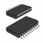 XC18V01SO20C0100
The activity of extra discounts on wholesale prices is in full swing…
Please fill in your contact information and we will send you the latest wholesale price list.





