 ChipApex | Global Electronic Components Supplier
SEARCH
Search Product
Search Post
— IC芯片 | 连接器 | 传感器 | 被动器件 —
Search productSearch post
— IC芯片 | 连接器 | 传感器 | 被动器件 —
Consult the customer manager about the wholesale price.
consultation hotline:86-132-6715-2157
email:[email protected]
Contact the product manager for consultation. One-stop consultation is available.
Do you want a lower wholesale price? Please send us your inquiry and we will reply immediately.
The AMD XCZU7EV-2FBVB900E is a Zynq UltraScale+ MPSoC System-on-Chip FPGA in a 900-ball FCBGA package. It integrates a quad-core ARM Cortex-A53 processor, dual-core ARM Cortex-R5 processor, and Mali-400 MP2 GPU. The device features 28,800 Adaptive Logic Modules (ALMs), 11 Mbit of embedded memory, and supports up to 220 I/Os. Operating at speed grade -2 with a maximum junction temperature of +100°C, it utilizes an 850 mV core voltage for high-performance embedded applications requiring mixed processing and programmable logic.
Verify the specific speed grade suffix (-2) against project timing requirements, as performance differs from -1 or -3 variants. Confirm RoHS compliance status and moisture sensitivity level (MSL) ratings prior to assembly planning. Ensure availability of compatible development boards and software licenses for the Zynq UltraScale+ MPSoC platform.
Select this model when a balance of moderate FPGA fabric size and robust application processor performance is required. Compare against the XCZU7EV-1 variant if higher clock frequencies are needed, or the XCZU4EG series if lower power consumption and reduced logic resources suffice. Validate that the 900-ball BGA footprint fits the target PCB design constraints.
This component belongs to the Zynq UltraScale+ MPSoC EV family, designed for cost-sensitive embedded markets. It shares the same silicon architecture as other EV devices but varies by speed bin and package. The part number indicates the specific electrical characteristics and thermal performance envelope defined by AMD for mass production.
Direct pin-to-pin replacements within the same package include other speed grades of the XCZU7EV series, such as XCZU7EV-1FBVB900E or XCZU7EV-3FBVB900E, provided timing closure can be met. Cross-family replacements like the XCZU5CG require significant schematic and layout modifications.
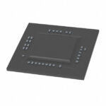 XCZU7EV-2FBVB900E
The activity of extra discounts on wholesale prices is in full swing…
Please fill in your contact information and we will send you the latest wholesale price list.




