 ChipApex | Global Electronic Components Supplier
SEARCH
Search Product
Search Post
— IC芯片 | 连接器 | 传感器 | 被动器件 —
Search productSearch post
— IC芯片 | 连接器 | 传感器 | 被动器件 —
Consult the customer manager about the wholesale price.
consultation hotline:86-132-6715-2157
email:[email protected]
Contact the product manager for consultation. One-stop consultation is available.
Do you want a lower wholesale price? Please send us your inquiry and we will reply immediately.
The ZL30631LDG1 is a system synchronizer featuring up to five independent clock channels, ten inputs, and twenty outputs. It supports any-to-any frequency conversion with input frequencies from 0.5 Hz to 1250 MHz and output frequencies from 0.5 Hz to 750 MHz. The device includes up to eight DPLLs for timing compliance with ITU-T G.8262 and G.813 standards. Output jitter is typically 100 fsRMS at 156.25 MHz (12 kHz to 20 MHz bandwidth). Core power consumption is less than 0.9W. It operates with 1.8V and 3.3V core VDD voltages and utilizes an SPI or I2C interface.
Verify the specific ordering suffix against the manufacturer's current product brief to confirm package type and temperature range. Ensure compatibility with required supply voltages (1.8V and 3.3V) and interface protocols (SPI/I2C). Confirm that the internal Flash memory configuration meets the application's power-up requirements without external components.
Select this component when requiring high-density clock distribution with flexible frequency conversion capabilities. The ZL30631 supports split-XO configurations using separate stability and jitter references to optimize cost. Verify that the required number of DPLLs and synthesizers fits within the five-channel limit. Check if the 1 ps phase adjustment resolution meets the system's alignment needs.
The ZL30631 is part of the ZL3063x family of system synchronizers, which also includes models ZL30632 through ZL30635. These devices share a common architecture but differ in the number of available DPLLs and synthesizer channels. The ZL30631 represents a specific configuration within this series designed for carrier-grade synchronization applications.
Direct replacements within the same family include ZL30632, ZL30633, ZL30634, and ZL30635. Selection depends on whether the additional DPLLs or synthesizer channels offered by higher-numbered models are necessary for the design.
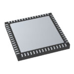 ZL30631LDG1
The activity of extra discounts on wholesale prices is in full swing…
Please fill in your contact information and we will send you the latest wholesale price list.





