 ChipApex | Global Electronic Components Supplier
SEARCH
Search Product
Search Post
— IC芯片 | 连接器 | 传感器 | 被动器件 —
Search productSearch post
— IC芯片 | 连接器 | 传感器 | 被动器件 —
Consult the customer manager about the wholesale price.
consultation hotline:86-132-6715-2157
email:[email protected]
Contact the product manager for consultation. One-stop consultation is available.
Do you want a lower wholesale price? Please send us your inquiry and we will reply immediately.
The ZL30645LDG1 is a line card timing IC from the ZL3064x family, designed for carrier-grade systems. It features up to five independent clock channels with any-to-any frequency conversion capabilities. The device supports up to 10 differential or single-ended inputs and provides up to 20 CMOS or 10 differential outputs. Key electrical parameters include an input frequency range of 1 kHz to 1250 MHz and an output frequency range of 0.5 Hz to 750 MHz. Typical output jitter is 100 fsRMS at 156.25 MHz. The core power consumption is less than 0.9W, and it operates with 1.8V and 3.3V core VDD voltages.
Verify the specific ordering suffix against the manufacturer's datasheet to confirm package type and temperature range. Ensure compatibility with required SPI/I2C interface configurations and internal Flash memory settings during procurement planning.
Select this model when up to five independent clock channels are required. Verify that the application needs support for up to 10 inputs and 20 outputs. Confirm that the local oscillator frequency requirements fall within the 9.72 MHz to 400 MHz range for optimal performance.
This component belongs to the ZL30641-ZL30645 product line, which offers scalable channel counts. The ZL30645 represents the highest configuration in this series with five channels, distinguishing it from lower-channel variants like the ZL30641 or ZL30642.
Check for other members of the ZL3064x family if fewer channels are sufficient. Verify pinout compatibility and software configuration scripts when substituting with other devices in the same product brief scope.
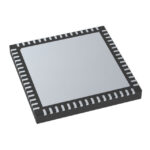 ZL30645LDG1
The activity of extra discounts on wholesale prices is in full swing…
Please fill in your contact information and we will send you the latest wholesale price list.






