 ChipApex | Global Electronic Components Supplier
SEARCH
Search Product
Search Post
— IC芯片 | 连接器 | 传感器 | 被动器件 —
Search productSearch post
— IC芯片 | 连接器 | 传感器 | 被动器件 —
Consult the customer manager about the wholesale price.
consultation hotline:86-132-6715-2157
email:[email protected]
Contact the product manager for consultation. One-stop consultation is available.
Do you want a lower wholesale price? Please send us your inquiry and we will reply immediately.
The EVVO 10N65F is a silicon N-channel enhancement mode VDMOSFET utilizing self-aligned planar technology to reduce conduction loss and improve switching performance. It features a 650V drain-source voltage rating and a continuous drain current of 10A. The device offers a maximum on-resistance of 0.9Ω at VGS=10V, with a typical value of 0.75Ω. Key electrical parameters include a total gate charge of 19nC, single pulse avalanche energy of 426mJ, and repetitive avalanche energy of 41mJ. Thermal resistance from junction-to-case is 4.46°C/W, while junction-to-ambient is 46.7°C/W. Operating temperature ranges from -55°C to +150°C.
Verify the specific ordering suffix against official documentation, as variations such as IP may indicate package or tape-and-reel configurations. Confirm RoHS compliance status directly with the manufacturer or authorized distributor lists. Ensure the component matches the required thermal and electrical specifications for the target application before procurement.
Select this component for high-voltage applications requiring low on-resistance and robust avalanche ruggedness. The 650V rating supports primary-side switching in offline converters. Consider the thermal resistance values when designing heatsinking solutions. The integrated body diode characteristics should be evaluated for synchronous rectification or flyback topologies.
This part belongs to the family of 650V N-channel power MOSFETs designed for medium-power switching applications. It utilizes planar DMOS technology common in modern power semiconductors to balance conduction losses with switching speed. The device is intended to replace older generation MOSFETs in AC-DC adapters, chargers, and industrial power supplies where efficiency and reliability are critical.
Cross-reference pinouts and thermal characteristics when substituting. Verify that alternative parts meet the 650V breakdown and 10A current requirements. Check if the replacement offers comparable avalanche energy ratings for robust operation in inductive load scenarios.
The maximum single pulse avalanche energy is 426 mJ under specified test conditions.
Yes, the transistor includes an integrated body diode with a continuous current rating of 9.0 A and a reverse recovery time of 431 ns.
The operating junction and storage temperature range is from -55°C to +150°C.
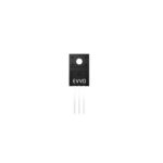 10N65F
The activity of extra discounts on wholesale prices is in full swing…
Please fill in your contact information and we will send you the latest wholesale price list.





