 ChipApex | Global Electronic Components Supplier
SEARCH
Search Product
Search Post
— IC芯片 | 连接器 | 传感器 | 被动器件 —
Search productSearch post
— IC芯片 | 连接器 | 传感器 | 被动器件 —
Consult the customer manager about the wholesale price.
consultation hotline:86-132-6715-2157
email:[email protected]
Contact the product manager for consultation. One-stop consultation is available.
Do you want a lower wholesale price? Please send us your inquiry and we will reply immediately.
The Renesas Electronics Corporation 23S09E-1DCGI8 is a 3.3V zero delay clock buffer featuring an integrated phase-locked loop (PLL). It distributes one reference input to nine outputs organized into two banks: five outputs in Bank A and four in Bank B. The device supports operating frequencies from 10MHz to 200MHz with a maximum output-to-output skew of 250ps and cycle-to-cycle jitter under 200ps. It operates within a supply voltage range of 3V to 3.6V and is housed in a 16-pin SOIC package. This specific variant provides standard drive capability and is characterized for industrial temperature ranges.
Verify the component status as the source indicates this part number may be obsolete or end-of-life. Confirm the manufacturer designation, as the datasheet originates from Integrated Device Technology (IDT), which was acquired by Renesas. Ensure the ordering suffix matches the required temperature grade and packaging format before procurement.
Select the -1H suffix if higher drive strength and faster rise/fall times (1.5ns) are required compared to the standard -1 drive. Verify that the load capacitance requirements align with the specified limits (30pF below 100MHz, 10pF above 100MHz). Ensure the design accommodates the 16-pin SOIC footprint and moisture sensitivity level 3.
This component belongs to the IDT23S09E family of high-speed PLL clock buffers. It serves as a 16-pin expansion of the 14-pin IDT23S05E, providing additional output channels. The device is designed to replace direct clock routing with buffered, low-skew signals in high-speed digital systems requiring precise timing synchronization.
Renesas recommends the 23S09-1HPGGI8 as a replacement for the 23S09E-1DCGI8.
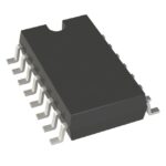 23S09E-1DCGI8
The activity of extra discounts on wholesale prices is in full swing…
Please fill in your contact information and we will send you the latest wholesale price list.





