 ChipApex | Global Electronic Components Supplier

SEARCH
Search Product
Search Post
— IC芯片 | 连接器 | 传感器 | 被动器件 —
Search productSearch post
— IC芯片 | 连接器 | 传感器 | 被动器件 —
Consult the customer manager about the wholesale price.
consultation hotline:86-132-6715-2157
email:[email protected]
Contact the product manager for consultation. One-stop consultation is available.
Do you want a lower wholesale price? Please send us your inquiry and we will reply immediately.
2N5116 is listed in the Jfets range at ChipApex. The manufacturer field lists Central Semiconductor Corp. Its product description is JFET P-CH 30V TO18. Review the specifications below when checking this part for your BOM.
The Central Semiconductor Corp 2N5116 is a silicon P-channel Junction Field-Effect Transistor (JFET) designed for switching applications. It operates in depletion mode and is housed in a TO-18 metal can package with three pins: Source, Gate, and Drain. The device supports an operating junction temperature range of -65°C to +200°C. Key electrical characteristics include a maximum gate-source voltage of 30V and a power dissipation rating of 500mW at 25°C ambient temperature. For the 2N5116 variant, the drain-source on-resistance (rDS(ON)) is specified as a maximum of 150Ω at ID=1.0mA and VGS=0V. The off-state drain current (ID(OFF)) is limited to 500pA under specific bias conditions.
Verify the specific plating configuration required for your assembly process before ordering. Central Semiconductor offers both Tin/Lead and Lead-Free options. To specify Tin/Lead plating, append the suffix "TIN/LEAD" to the part number. For Lead-Free compliance, use the suffix "PBFREE". Confirm that the selected variant meets your environmental regulations and soldering profile requirements.
Select the 2N5116 when a P-channel JFET with a wide operating temperature range is needed. Ensure the circuit design accommodates the maximum ratings of 30V for both Gate-Drain and Gate-Source voltages. Verify that the load current does not exceed the device's power dissipation capabilities within the thermal constraints of the TO-18 package.
The 2N5116 belongs to a family of silicon P-channel JFETs manufactured by Central Semiconductor Corp, which also includes the 2N5114 and 2N5115. These devices share the same physical TO-18 case outline but differ in their electrical parameter bins, such as pinch-off voltage and on-resistance. This component is distinct from other transistor types like BJTs or MOSFETs due to its depletion-mode operation and high input impedance.
Central Semiconductor has listed the 2N5115 as End of Life with no suggested replacement available. No direct substitute part numbers are officially documented for the 2N5116 in the provided datasheet or product discontinuation notices. Engineers should consult application engineering support for potential alternate sources if this component becomes unavailable.
The lead code for the TO-18 case is defined as Pin 1 being the Source, Pin 2 being the Gate, and Pin 3 being the Drain.
While all three devices share the same physical package and basic structure, they are distinguished by their electrical characteristic bins. The 2N5116 has specific limits for parameters such as IDSS (5.0 to 25 mA) and VGS(OFF) (1.0 to 4.0 V) that differ from the other variants.
The maximum operating and storage junction temperature (Tj, Tstg) for the 2N5116 is +200°C.
Explore related parts through Transistors, Discrete Semiconductor Products, all product categories, ChipApex homepage.
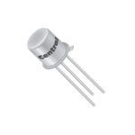 2N5116

The activity of extra discounts on wholesale prices is in full swing…
Please fill in your contact information and we will send you the latest wholesale price list.





