 ChipApex | Global Electronic Components Supplier
SEARCH
Search Product
Search Post
— IC芯片 | 连接器 | 传感器 | 被动器件 —
Search productSearch post
— IC芯片 | 连接器 | 传感器 | 被动器件 —
Consult the customer manager about the wholesale price.
consultation hotline:86-132-6715-2157
email:[email protected]
Contact the product manager for consultation. One-stop consultation is available.
Do you want a lower wholesale price? Please send us your inquiry and we will reply immediately.
The Microchip Technology 2N7000-G is an N-Channel Enhancement-Mode Vertical DMOS FET housed in a 3-lead TO-92 through-hole package. It features a Drain-to-Source Voltage (BVDSS) of 60 V and a maximum Gate-to-Source Voltage of ±30 V. The device provides a continuous On-State Drain Current (ID(ON)) of 75 mA at VGS = 4.5 V, with a peak pulsed current capability of 500 mA. Static Drain-to-Source On-State Resistance (RDS(ON)) is specified at a maximum of 5 Ω at VGS = 10 V. The Gate Threshold Voltage (VGS(th)) ranges from 0.8 V to 3 V. Operating ambient temperature spans from -55°C to +150°C.
Verify that the ordering suffix '-G' corresponds to the lead-free/RoHS-compliant variant as defined in the product identification system. Confirm the media type matches the required packaging quantity, typically 1000 per bag for this specific part number configuration. Ensure the component meets the environmental specifications required for the target operating temperature range.
Select this component when a normally-off N-channel switch is required with high input impedance and robust thermal stability. The vertical DMOS technology ensures freedom from thermal runaway. Consider the 5 ohm on-state resistance and 75 mA continuous current limit when designing load circuits. Verify that the gate threshold voltage aligns with the available control logic voltage levels.
This device utilizes a well-proven silicon gate manufacturing process combined with a vertical DMOS structure. This architecture delivers power handling capabilities comparable to bipolar transistors while maintaining the high input impedance characteristic of MOS devices. The design is optimized for applications requiring very low threshold voltage, high breakdown voltage, and fast switching speeds.
Cross-reference with other manufacturers offering the standard 2N7000 specification in a TO-92 package. Verify pinout compatibility and ensure electrical parameters such as RDS(ON), BVDSS, and VGS(th) meet or exceed the requirements of the original design.
The absolute maximum rating for Gate-to-Source Voltage is ±30 V.
Yes, the device is free from thermal runaway and thermally induced secondary breakdown due to its positive temperature coefficient.
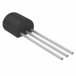 2N7000-G
The activity of extra discounts on wholesale prices is in full swing…
Please fill in your contact information and we will send you the latest wholesale price list.





