 ChipApex | Global Electronic Components Supplier
SEARCH
Search Product
Search Post
— IC芯片 | 连接器 | 传感器 | 被动器件 —
Search productSearch post
— IC芯片 | 连接器 | 传感器 | 被动器件 —
Consult the customer manager about the wholesale price.
consultation hotline:86-132-6715-2157
email:[email protected]
Contact the product manager for consultation. One-stop consultation is available.
Do you want a lower wholesale price? Please send us your inquiry and we will reply immediately.
The Nexperia 2N7002BKV is a dual N-channel enhancement mode Field-Effect Transistor utilizing Trench MOSFET technology. It is housed in an ultra-small SOT666 surface-mounted plastic package with a 0.5 mm pitch and dimensions of 1.6 mm x 1.2 mm x 0.55 mm. The device provides two independent channels, each rated for a drain-source voltage of 60 V and a continuous drain current of 340 mA at 25 °C. Key electrical characteristics include a maximum gate-source voltage of ±20 V, a typical on-state resistance of 1 Ω at VGS = 10 V, and a total gate charge of 0.5 nC. The component supports junction temperatures up to 150 °C and includes electrostatic discharge protection exceeding 2 kV HBM.
Verify the specific ordering suffix against official Nexperia documentation to confirm the exact package variant and reel specifications. Ensure that the procurement channel sources products directly from authorized distributors or the manufacturer to guarantee authenticity. Cross-reference the marking code 'ZG' with the latest datasheet revision to validate the component identity upon receipt.
Select this component when space-constrained designs require dual N-channel switching capabilities within the SOT666 footprint. The low on-state resistance and high threshold voltage compatibility make it suitable for applications requiring efficient signal switching driven by standard logic levels. Evaluate thermal dissipation requirements carefully, as the small package size limits power handling compared to larger packages.
This part belongs to Nexperia's Trench MOSFET series, which utilizes proprietary trench gate technology to optimize switching speed and conduction losses. The 2N7002BKV specifically addresses the need for compact dual-channel solutions in portable electronics and dense printed circuit board layouts where individual single-channel transistors would consume excessive board area.
Publicly confirmed substitute part numbers are not available in the provided source material.
Pin 1 is Source 1, Pin 2 is Gate 1, Pin 3 is Drain 2, Pin 4 is Source 2, Pin 5 is Gate 2, and Pin 6 is Drain 1.
The maximum peak drain current (IDM) is 1.2 A for a single pulse duration of 10 µs or less at 25 °C.
The device features integrated ESD protection capable of withstanding up to 2 kV according to the Human Body Model (HBM) testing standard.
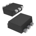 2N7002BKV,115
The activity of extra discounts on wholesale prices is in full swing…
Please fill in your contact information and we will send you the latest wholesale price list.





