 ChipApex | Global Electronic Components Supplier
SEARCH
Search Product
Search Post
— IC芯片 | 连接器 | 传感器 | 被动器件 —
Search productSearch post
— IC芯片 | 连接器 | 传感器 | 被动器件 —
Consult the customer manager about the wholesale price.
consultation hotline:86-132-6715-2157
email:[email protected]
Contact the product manager for consultation. One-stop consultation is available.
Do you want a lower wholesale price? Please send us your inquiry and we will reply immediately.
The Toshiba 2SJ438 is a silicon P-channel MOS field-effect transistor utilizing L²-π-MOSV technology. It features a low drain-source ON resistance of 0.16 Ω (typical) and high forward transfer admittance of 4.0 S (typical). The device supports 4-V gate drive with an enhancement mode threshold voltage ranging from -0.8 V to -2.0 V. Absolute maximum ratings include a drain-source voltage of -60 V, continuous DC drain current of -5 A, and pulse drain current of -20 A. Power dissipation reaches 25 W at 25°C case temperature.
Verify the specific ordering suffix against official Toshiba documentation to confirm environmental compliance status, such as RoHS compatibility. Confirm package type JEDEC SC-67 availability. Review the Toshiba Semiconductor Reliability Handbook for derating concepts and methods before finalizing designs. Ensure channel temperature limits are respected during operation.
Select this component for applications requiring efficient switching with low conduction losses. The device is suitable for general electronics including computers and industrial robots. Verify that the design accounts for the absolute maximum ratings, particularly regarding avalanche energy and thermal resistance. Ensure electrostatic discharge precautions are implemented during handling due to device sensitivity.
This part belongs to the Toshiba Silicon P Channel MOS Type series. It is designed for general electronics applications. The manufacturer reserves the right to make changes without notice. The product is not intended for use in nuclear facilities, aerospace, medical equipment, or other unintended uses requiring extraordinary reliability levels.
Public confirmed substitute part numbers are not available in the provided datasheet.
The typical drain-source ON resistance is 0.16 Ω when VGS is -4 V and ID is -2.5 A.
The maximum continuous DC drain current is -5 A at a case temperature of 25°C.
The gate threshold voltage ranges from -0.8 V to -2.0 V under test conditions of VDS = -10 V and ID = -1 mA.
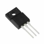 2SJ438(AISIN,Q,M)
The activity of extra discounts on wholesale prices is in full swing…
Please fill in your contact information and we will send you the latest wholesale price list.





