 ChipApex | Global Electronic Components Supplier
SEARCH
Search Product
Search Post
— IC芯片 | 连接器 | 传感器 | 被动器件 —
Search productSearch post
— IC芯片 | 连接器 | 传感器 | 被动器件 —
Consult the customer manager about the wholesale price.
consultation hotline:86-132-6715-2157
email:[email protected]
Contact the product manager for consultation. One-stop consultation is available.
Do you want a lower wholesale price? Please send us your inquiry and we will reply immediately.
The Toshiba 2SJ438 is a silicon P-channel enhancement-mode MOSFET designed for general-purpose power switching. It features a maximum drain-source voltage of -60 V and a continuous DC drain current rating of -5 A. The device exhibits a typical drain-source on-resistance of 0.16 Ω at VGS = -10 V, with a maximum gate threshold voltage range of -0.8 to -2.0 V. Packaged in the JEDEC SC-67 (TOSHIBA 2-10R1B) format, it provides a thermal resistance from channel to case of 5.0 °C/W.
Verify component authenticity by checking the marking code 'J438' against the lot number format specified in the datasheet. Confirm RoHS compatibility status through official Toshiba sales representatives, as indicated by the presence or absence of an underline under the lot number. Ensure handling procedures account for electrostatic sensitivity during assembly.
Select this component when a P-channel MOSFET with a -60 V breakdown voltage and -5 A continuous current capability is required. Consider the 0.16 Ω typical on-resistance for low-loss switching applications. Evaluate the thermal performance using the provided junction-to-case resistance values to ensure adequate heat dissipation within the specified 150°C channel temperature limit.
This device belongs to Toshiba's L²-π-MOSV series of silicon P-channel field effect transistors. It utilizes specific MOS technology optimized for power switching efficiency. The component is intended for general electronics applications such as computers, office equipment, and industrial robots, excluding high-reliability sectors like aerospace or medical devices unless explicitly permitted.
No public substitute part numbers are documented in the source material.
The absolute maximum rating for gate-source voltage is ±20 V.
Yes, the device includes a Source-Drain diode with a maximum forward voltage of 1.7 V at -5 A.
The transistor is housed in the JEDEC SC-67 package, also designated as TOSHIBA 2-10R1B.
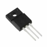 2SJ438,Q(M
The activity of extra discounts on wholesale prices is in full swing…
Please fill in your contact information and we will send you the latest wholesale price list.





