 ChipApex | Global Electronic Components Supplier
SEARCH
Search Product
Search Post
— IC芯片 | 连接器 | 传感器 | 被动器件 —
Search productSearch post
— IC芯片 | 连接器 | 传感器 | 被动器件 —
Consult the customer manager about the wholesale price.
consultation hotline:86-132-6715-2157
email:[email protected]
Contact the product manager for consultation. One-stop consultation is available.
Do you want a lower wholesale price? Please send us your inquiry and we will reply immediately.
The Toshiba Semiconductor and Storage 2SK1119(F) is a silicon N-channel MOSFET utilizing π-MOS II.5 technology, housed in a TO-220AB package. It features a drain-source voltage of 1000 V and a continuous drain current of 4 A at 25°C case temperature. The device exhibits a typical drain-source ON resistance of 3.0 Ω and a forward transfer admittance of 2.0 S. Key electrical characteristics include a gate threshold voltage range of 1.5 to 3.5 V and a maximum drain cut-off current of 300 μA at 800 V. Thermal performance includes a channel-to-case thermal resistance of 1.25 °C/W.
Verify the specific suffix designation against official Toshiba documentation to confirm environmental compliance status, as markings indicate RoHS compatibility distinctions. Confirm that the component meets all absolute maximum ratings for your operating conditions, particularly regarding channel temperature limits and power dissipation derating requirements.
Select this component for designs requiring high-voltage isolation and efficient power switching. Ensure the application circuit accounts for the specified thermal resistance and provides adequate heat sinking to maintain the channel temperature within the 150°C limit during continuous operation under load.
This device belongs to the Toshiba π-MOS II.5 series of silicon N-channel MOSFETs. These transistors are engineered for general electronics applications, offering a balance of high voltage handling and low on-state resistance suitable for power management tasks.
Publicly confirmed substitute part numbers are not available in the provided source material.
The absolute maximum drain-source voltage (VDSS) is rated at 1000 V.
The gate threshold voltage (Vth) ranges from 1.5 V to 3.5 V, measured at a drain-source voltage of 10 V and a drain current of 1 mA.
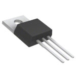 2SK1119(F)
The activity of extra discounts on wholesale prices is in full swing…
Please fill in your contact information and we will send you the latest wholesale price list.





