 ChipApex | Global Electronic Components Supplier
SEARCH
Search Product
Search Post
— IC芯片 | 连接器 | 传感器 | 被动器件 —
Search productSearch post
— IC芯片 | 连接器 | 传感器 | 被动器件 —
Consult the customer manager about the wholesale price.
consultation hotline:86-132-6715-2157
email:[email protected]
Contact the product manager for consultation. One-stop consultation is available.
Do you want a lower wholesale price? Please send us your inquiry and we will reply immediately.
The onsemi 2SK2394-7-TB-E is an N-channel JFET in a CP3 (SC-59-3) surface-mount package. It operates with a Drain-to-Source Voltage of 15 V and supports a maximum Drain Current of 50 mA. The device provides a Drain Current (IDSS) range of 10 to 20 mA at VDS = 5 V, with a Forward Transfer Admittance (|yfs|) ranging from 20 to 38 mS. Key electrical parameters include a Gate Cutoff Voltage (VGS(off)) between -0.3 V and -1.0 V, Input Capacitance (Ciss) of 10 pF, and Reverse Transfer Capacitance (Crss) of 2.9 pF. It features a low Noise Figure of 1.0 dB at 1 kHz.
Verify the specific ordering suffix against official documentation to confirm packaging details. Confirm RoHS compliance status directly with the manufacturer or authorized distributors before procurement. Ensure the component meets all environmental and safety standards required for the intended application environment.
Select this component when ultralow noise performance and high transconductance are critical requirements. The 10–20 mA IDSS range offers flexibility for biasing configurations. Verify that the 15 V voltage rating aligns with the system's maximum operating conditions to ensure reliable operation within absolute maximum ratings.
This part belongs to the 2SK2394 family of N-channel JFETs manufactured by onsemi. It is designed specifically for applications requiring high gain and minimal noise introduction in compact form factors. The device utilizes a lead-free manufacturing process consistent with modern environmental regulations.
Consult official substitution guides for verified alternatives. Cross-compatibility depends on matching IDSS ranges, voltage ratings, and package dimensions. Verify pinout alignment and thermal characteristics before implementing any substitute components in existing designs.
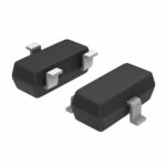 2SK2394-7-TB-E
The activity of extra discounts on wholesale prices is in full swing…
Please fill in your contact information and we will send you the latest wholesale price list.





