 ChipApex | Global Electronic Components Supplier
SEARCH
Search Product
Search Post
— IC芯片 | 连接器 | 传感器 | 被动器件 —
Search productSearch post
— IC芯片 | 连接器 | 传感器 | 被动器件 —
Consult the customer manager about the wholesale price.
consultation hotline:86-132-6715-2157
email:[email protected]
Contact the product manager for consultation. One-stop consultation is available.
Do you want a lower wholesale price? Please send us your inquiry and we will reply immediately.
The Toshiba 2SK2507 is a silicon N-channel MOS field-effect transistor utilizing L2-π-MOSV technology. It features a low drain-source ON resistance of 0.034 Ω (typical) at VGS = 10 V and ID = 12 A, alongside a high forward transfer admittance of 16 S (typical). The device supports 4-V gate drive with an enhancement mode threshold voltage ranging from 0.8 to 2.0 V. Absolute maximum ratings include a 50 V drain-source voltage, 25 A DC drain current, and 30 W power dissipation at 25°C case temperature.
Verify the specific ordering suffix against official Toshiba Semiconductor and Storage documentation to confirm environmental compliance status, such as RoHS compatibility or lead-free designation. Confirm package markings and lot number formatting requirements before finalizing procurement specifications.
Select this component for designs requiring low conduction losses and fast switching speeds in moderate-voltage environments. Ensure thermal management strategies account for the specified channel-to-case thermal resistance. Validate that the application operates within the absolute maximum ratings for avalanche energy and repetitive pulse currents.
This part belongs to Toshiba's N-channel MOSFET portfolio designed for general-purpose switching applications. It utilizes advanced π-MOSV architecture to optimize the trade-off between on-resistance and gate charge, making it suitable for compact power supply and motor control implementations.
Consult official Toshiba substitution guides for verified equivalents. Cross-referencing requires matching key parameters such as RDS(ON), V(BR)DSS, and package dimensions to ensure functional compatibility without design modification.
The typical forward transfer admittance (|Yfs|) is 16 S when measured at VDS = 10 V and ID = 12 A.
Yes, the device supports single-pulse avalanche energy up to 138 mJ under specific test conditions including VDD = 25 V and RG = 25 Ω.
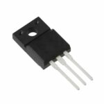 2SK2507(F)
The activity of extra discounts on wholesale prices is in full swing…
Please fill in your contact information and we will send you the latest wholesale price list.





