ChipApex | Global Electronic Components Supplier
SEARCH
Search Product
Search Post
— IC芯片 | 连接器 | 传感器 | 被动器件 —
Search productSearch post
— IC芯片 | 连接器 | 传感器 | 被动器件 —
Consult the customer manager about the wholesale price.
consultation hotline:86-132-6715-2157
email:[email protected]
Contact the product manager for consultation. One-stop consultation is available.
Do you want a lower wholesale price? Please send us your inquiry and we will reply immediately.
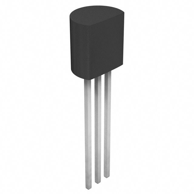
The Toshiba 2SK2989 is a silicon N-channel MOS field-effect transistor utilizing π-MOSVI technology. It features a low drain-source ON resistance of 120 mΩ (typical) at VGS = 10 V and ID = 2.5 A, alongside a high forward transfer admittance of 2.6 S. The device supports a maximum drain-source voltage of 50 V and continuous DC drain current of 5 A. It operates within a channel temperature range up to 150°C and is housed in a JEDEC TO-92MOD package.
Verify the specific ordering suffix against the manufacturer's documentation to confirm environmental compliance status, such as RoHS compatibility. Confirm that the component is suitable for general electronics applications and not intended for unintended uses requiring extraordinary reliability levels. Ensure proper handling precautions are observed due to electrostatic sensitivity.
Select this component for applications requiring low conduction losses and fast switching characteristics within a 50 V voltage rating. Consider the thermal resistance of 138 °C/W when designing heat dissipation strategies for the TO-92MOD package. Evaluate the gate threshold voltage range of 1.0 to 2.2 V to ensure compatibility with the driving logic levels.
This part belongs to the family of silicon N-channel MOSFETs manufactured by Toshiba Semiconductor and Storage. It is designed using the π-MOSVI process technology, which optimizes the trade-off between ON resistance and switching speed. The device is packaged in a standard TO-92MOD form factor suitable for surface mount or through-hole integration depending on the specific board design.
Consult official Toshiba documentation for verified substitute part numbers. Do not assume cross-compatibility with other manufacturers' devices without verifying pinout, electrical ratings, and package dimensions.
 2SK2989(T6CANO,F,M
The activity of extra discounts on wholesale prices is in full swing…
Please fill in your contact information and we will send you the latest wholesale price list.