ChipApex | Global Electronic Components Supplier
SEARCH
Search Product
Search Post
— IC芯片 | 连接器 | 传感器 | 被动器件 —
Search productSearch post
— IC芯片 | 连接器 | 传感器 | 被动器件 —
Consult the customer manager about the wholesale price.
consultation hotline:86-132-6715-2157
email:[email protected]
Contact the product manager for consultation. One-stop consultation is available.
Do you want a lower wholesale price? Please send us your inquiry and we will reply immediately.
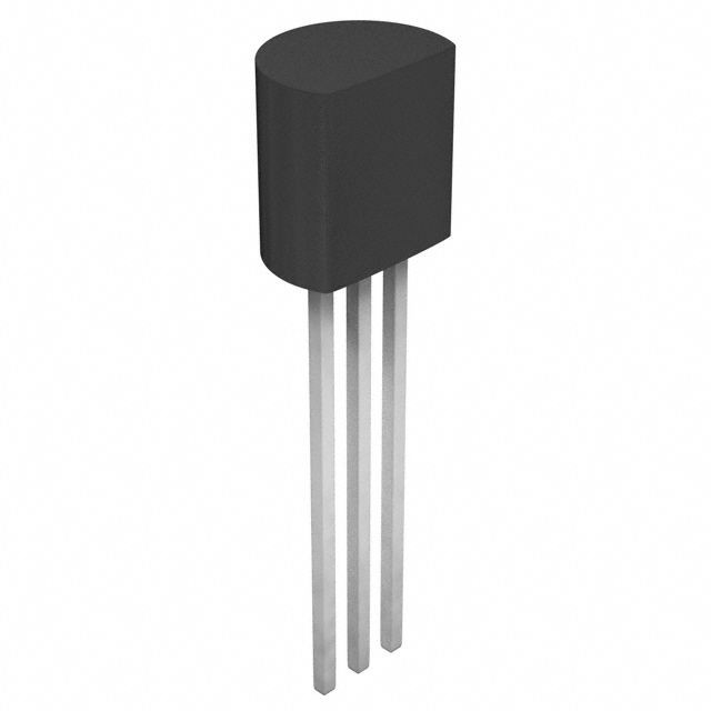
The Toshiba 2SK2989 is a silicon N-channel MOS field-effect transistor utilizing π-MOSVI technology, designed for chopper regulators, DC-DC converters, and motor drive applications. It features a low drain-source ON resistance of 120 mΩ (typical) at VGS=10V and ID=2.5A, alongside a high forward transfer admittance of 2.6 S. The device operates with a drain-source voltage rating of 50V and supports continuous drain currents up to 5A. Key electrical characteristics include a gate threshold voltage range of 1.0 to 2.2V and a maximum leakage current of 100 μA.
Verify the specific ordering suffix J(T6F) against official Toshiba Semiconductor and Storage documentation to confirm package type and environmental compliance status. Ensure that design parameters remain within absolute maximum ratings, particularly regarding channel temperature limits and thermal resistance derating curves. Consult the manufacturer's reliability handbook for appropriate handling precautions and electrostatic discharge protection measures during assembly.
Select this component when designing low-voltage power stages requiring efficient switching with minimal conduction losses. The 50V rating suits applications where input voltages are moderate, while the TO-92MOD package offers a compact footprint for space-constrained boards. Evaluate thermal management requirements based on the specified junction-to-ambient thermal resistance to ensure reliable operation under continuous load conditions.
This part belongs to Toshiba's discrete semiconductor lineup focusing on general-purpose switching applications. The π-MOSVI process technology distinguishes it by offering optimized trade-offs between ON resistance and switching speed. It serves as a fundamental building block in power management integrated circuits and standalone driver stages within consumer electronics and industrial control equipment.
Consult official Toshiba cross-reference lists for verified substitutes. Ensure any replacement maintains compatible pinout configurations, voltage ratings, and thermal characteristics suitable for the existing PCB layout and cooling infrastructure.
 2SK2989,T6F(J
The activity of extra discounts on wholesale prices is in full swing…
Please fill in your contact information and we will send you the latest wholesale price list.