 ChipApex | Global Electronic Components Supplier
SEARCH
Search Product
Search Post
— IC芯片 | 连接器 | 传感器 | 被动器件 —
Search productSearch post
— IC芯片 | 连接器 | 传感器 | 被动器件 —
Consult the customer manager about the wholesale price.
consultation hotline:86-132-6715-2157
email:[email protected]
Contact the product manager for consultation. One-stop consultation is available.
Do you want a lower wholesale price? Please send us your inquiry and we will reply immediately.
The Toshiba Semiconductor and Storage 2SK3462(TE16L1,NQ) is a silicon N-channel MOS type field effect transistor utilizing π-MOSV technology. It features a drain-source voltage rating of 250 V and a continuous DC drain current of 3 A. The device exhibits a typical drain-source ON-resistance of 1.2 Ω at VGS = 10 V and ID = 1.5 A, with a maximum of 1.7 Ω. It supports a 4 V gate drive and has a typical forward transfer admittance of 2.2 S. The component operates within a channel temperature range up to 150 °C and includes an internal body diode with a reverse recovery time of 125 ns.
Verify the specific ordering suffix TE16L1,NQ against official Toshiba documentation to confirm packaging and environmental compliance details. Ensure that the selected variant matches the required thermal resistance and package dimensions for your PCB layout. Cross-reference the datasheet revision date to confirm the accuracy of electrical parameters before finalizing procurement specifications.
Select this component for applications requiring a 250 V breakdown voltage and moderate current handling up to 3 A. Consider the 1.2 Ω typical ON-resistance for power loss calculations in switching regulators. Verify that the 4 V gate drive capability aligns with your controller's output levels. Evaluate the thermal management requirements based on the 6.25 °C/W thermal resistance from channel to case.
This part belongs to the 2SK3462 series of N-channel MOSFETs designed by Toshiba Semiconductor and Storage. It is engineered for general electronics applications such as computers, office equipment, and industrial robots. The device is distinct from automotive-grade parts like the TK33S10N1L, focusing instead on standard switching performance without explicit automotive qualification markings in the provided text.
No public confirmed substitute part numbers are available in the source material.
The absolute maximum drain-source voltage (VDSS) is rated at 250 V.
Yes, the datasheet specifies Source-Drain Ratings and Characteristics, including a forward voltage and reverse recovery time for the internal diode.
The gate threshold voltage (Vth) ranges from 1.5 V to 3.5 V when measured at VDS = 10 V and ID = 1 mA.
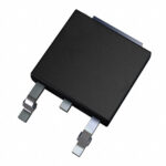 2SK3462(TE16L1,NQ)
The activity of extra discounts on wholesale prices is in full swing…
Please fill in your contact information and we will send you the latest wholesale price list.





