 ChipApex | Global Electronic Components Supplier
8T49N205-001NLGI8
Search Product
Search Post
— IC芯片 | 连接器 | 传感器 | 被动器件 —
Search productSearch post
— IC芯片 | 连接器 | 传感器 | 被动器件 —
Consult the customer manager about the wholesale price.
consultation hotline:86-132-6715-2157
email:[email protected]
Contact the product manager for consultation. One-stop consultation is available.
Do you want a lower wholesale price? Please send us your inquiry and we will reply immediately.
The 8T49N205-001NLGI8 is a frequency translator IC manufactured by Renesas Electronics Corporation. It operates with a maximum output frequency of 1.3 GHz and features a single output channel. The device is housed in a 40-VFQFN package with an exposed pad, designed for thermal efficiency and compact board space. It integrates a Phase-Locked Loop (PLL) with a bypass option to support flexible clock generation and jitter attenuation applications.
Verify the exact suffix '8' against the manufacturer's official documentation to confirm pinout, electrical characteristics, and environmental compliance. Suffixes often denote specific packaging or material variations that impact integration. Cross-reference the datasheet revision date to ensure alignment with current design specifications and avoid discrepancies in interface definitions.
Select this component when a 1.3 GHz frequency translation solution with LVDS/LVPECL outputs is required. Ensure the system design accommodates the 40-VFQFN package thermal requirements. Confirm that the input clock source matches the device's operational range and that the integrated PLL meets the specific jitter performance targets of the application.
This part belongs to the 8T49N series of programmable clock generators and jitter attenuators from Renesas. These devices are engineered for high-performance timing applications, offering low phase noise and flexible configuration options. The series supports various output formats and frequencies, making it suitable for complex digital systems requiring stable clock signals.
Consult the official cross-reference list for direct substitutes. Verify that any alternative part maintains identical output voltage levels, package dimensions, and functional capabilities to ensure seamless integration without redesigning the PCB layout.
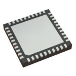 8T49N205-001NLGI8
The activity of extra discounts on wholesale prices is in full swing…
Please fill in your contact information and we will send you the latest wholesale price list.







