 ChipApex | Global Electronic Components Supplier
8T49N240-027NLGI8
Search Product
Search Post
— IC芯片 | 连接器 | 传感器 | 被动器件 —
Search productSearch post
— IC芯片 | 连接器 | 传感器 | 被动器件 —
Consult the customer manager about the wholesale price.
consultation hotline:86-132-6715-2157
email:[email protected]
Contact the product manager for consultation. One-stop consultation is available.
Do you want a lower wholesale price? Please send us your inquiry and we will reply immediately.
The Renesas 8T49N240-027NLGI8 is a FemtoClock jitter attenuator and clock synthesizer designed for high-performance timing applications. It operates within a supply voltage range of 2.375 V to 3.465 V, consuming approximately 40 mA of operating current. The device supports a maximum input frequency of 875 MHz and delivers outputs up to 867 MHz across four output channels. Packaged in a 6x6 mm VFQFPN-40 (VFQFN-40) surface-mount format, it functions reliably between -40°C and +85°C. This component integrates programmable features for precise clock generation and noise reduction.
Verify the specific suffix '027' against the official datasheet to confirm the exact frequency configuration and pinout, as suffixes define functional parameters. Confirm moisture sensitivity level (MSL) handling requirements prior to assembly. Check current availability status, as distribution may be limited or subject to factory special orders.
Select this component when a low-phase-noise solution is required for synthesizing multiple clock signals from a single reference. Ensure the design accommodates the 40 mA typical current draw and the 6x6 mm VFQFN-40 footprint. Validate that the required output frequencies fall within the 867 MHz limit and that the input reference does not exceed 875 MHz.
This part belongs to the Renesas FemtoClock 8T49N240 series, which specializes in ultra-low jitter performance. The 8T49N240 family provides flexible programming options for various clock topologies. The 'NLGI8' suffix typically indicates lead-free packaging and RoHS compliance, consistent with modern environmental standards for electronic components.
Direct replacements require matching the 4-output architecture and similar jitter specifications. Verify compatibility with the 8T49N240 series variants. Cross-reference electrical parameters such as supply voltage and package dimensions to ensure physical and functional interchangeability without redesigning the PCB layout.
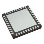 8T49N240-027NLGI8
The activity of extra discounts on wholesale prices is in full swing…
Please fill in your contact information and we will send you the latest wholesale price list.





