 ChipApex | Global Electronic Components Supplier
8T49N287A-999NLGI8
Search Product
Search Post
— IC芯片 | 连接器 | 传感器 | 被动器件 —
Search productSearch post
— IC芯片 | 连接器 | 传感器 | 被动器件 —
Consult the customer manager about the wholesale price.
consultation hotline:86-132-6715-2157
email:[email protected]
Contact the product manager for consultation. One-stop consultation is available.
Do you want a lower wholesale price? Please send us your inquiry and we will reply immediately.
The Renesas 8T49N287A-999NLGI8 is a FemtoClock NG octal frequency translator IC featuring two fractional-feedback PLLs. It supports input frequencies up to 1GHz and provides eight differential outputs. The device operates on dual supply voltages of 2.375V–2.625V and 3.135V–3.465V. It utilizes a 56-VFQFN exposed pad package with dimensions of 8x8mm. Output skew is specified at 45ps, supporting LVCMOS, LVDS, LVPECL, and HCSL output types.
Verify the specific suffix '999' against the official datasheet to confirm factory programming settings, as this variant defines unique output configurations. Confirm RoHS compliance status through manufacturer documentation. Ensure the 56-VFQFN package footprint matches the design layout requirements before procurement.
Select this component when dual independent PLLs are required for separate clock domains within a single package. The 1GHz maximum input frequency accommodates high-speed reference sources. Verify that the available output voltage levels (2.5V or 3.3V) align with the target load requirements.
This part belongs to the FemtoClock NG series, which focuses on low-jitter clock synthesis. The 8T49N287 family specifically offers octal outputs derived from two internal PLLs. This model represents a pre-programmed version of the programmable frequency translator, simplifying integration for standard applications.
The 8T49N287A-998NLGI8 is a documented substitute within the same series. Verify pin compatibility and electrical specifications before substitution. Other variants in the 8T49N287 family may require reprogramming or offer different output counts.
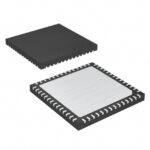 8T49N287A-999NLGI8
The activity of extra discounts on wholesale prices is in full swing…
Please fill in your contact information and we will send you the latest wholesale price list.





