ChipApex | Global Electronic Components Supplier
8V19N490-24BDGI
Search Product
Search Post
— IC芯片 | 连接器 | 传感器 | 被动器件 —
Search productSearch post
— IC芯片 | 连接器 | 传感器 | 被动器件 —
Consult the customer manager about the wholesale price.
consultation hotline:86-132-6715-2157
email:[email protected]
Contact the product manager for consultation. One-stop consultation is available.
Do you want a lower wholesale price? Please send us your inquiry and we will reply immediately.
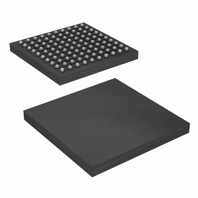
The 8V19N490-24BDGI is a FemtoClock NG Jitter Attenuator and Clock Synthesizer manufactured by Renesas Electronics. It features an 18-output architecture capable of generating frequencies up to 2.94912 GHz. The device supports LVDS and LVPECL output levels, with input levels compatible with LVDS and LVPECL standards. It operates on a maximum supply voltage of 3.3 V and utilizes a CABGA-100 surface-mount package. The component belongs to the 8V19N490A series and is classified as an integer clock synthesizer.
Mouser currently lists this part number as not supplied, indicating limited availability or factory special order status. Verification of current stock and lead times should be conducted directly with authorized distributors or the manufacturer before procurement planning.
Select this component for designs requiring high-output count clock synthesis with femtosecond jitter attenuation. Ensure the PCB layout accommodates the CABGA-100 package dimensions and that the system power supply provides a stable 3.3 V rail. Verify compatibility with LVDS/LVPECL signaling requirements for both inputs and outputs.
This device is part of the FemtoClock NG family, designed for high-performance clock conditioning. It integrates a two-stage PLL architecture to provide both jitter attenuation and frequency multiplication capabilities for demanding digital applications.
Publicly confirmed substitute part numbers are not available in the provided documentation. Consult Renesas technical support for cross-reference recommendations if this specific model is unavailable.
 8V19N490-24BDGI
The activity of extra discounts on wholesale prices is in full swing…
Please fill in your contact information and we will send you the latest wholesale price list.