ChipApex | Global Electronic Components Supplier
9FGV1005A000LTGI8
Search Product
Search Post
— IC芯片 | 连接器 | 传感器 | 被动器件 —
Search productSearch post
— IC芯片 | 连接器 | 传感器 | 被动器件 —
Consult the customer manager about the wholesale price.
consultation hotline:86-132-6715-2157
email:[email protected]
Contact the product manager for consultation. One-stop consultation is available.
Do you want a lower wholesale price? Please send us your inquiry and we will reply immediately.
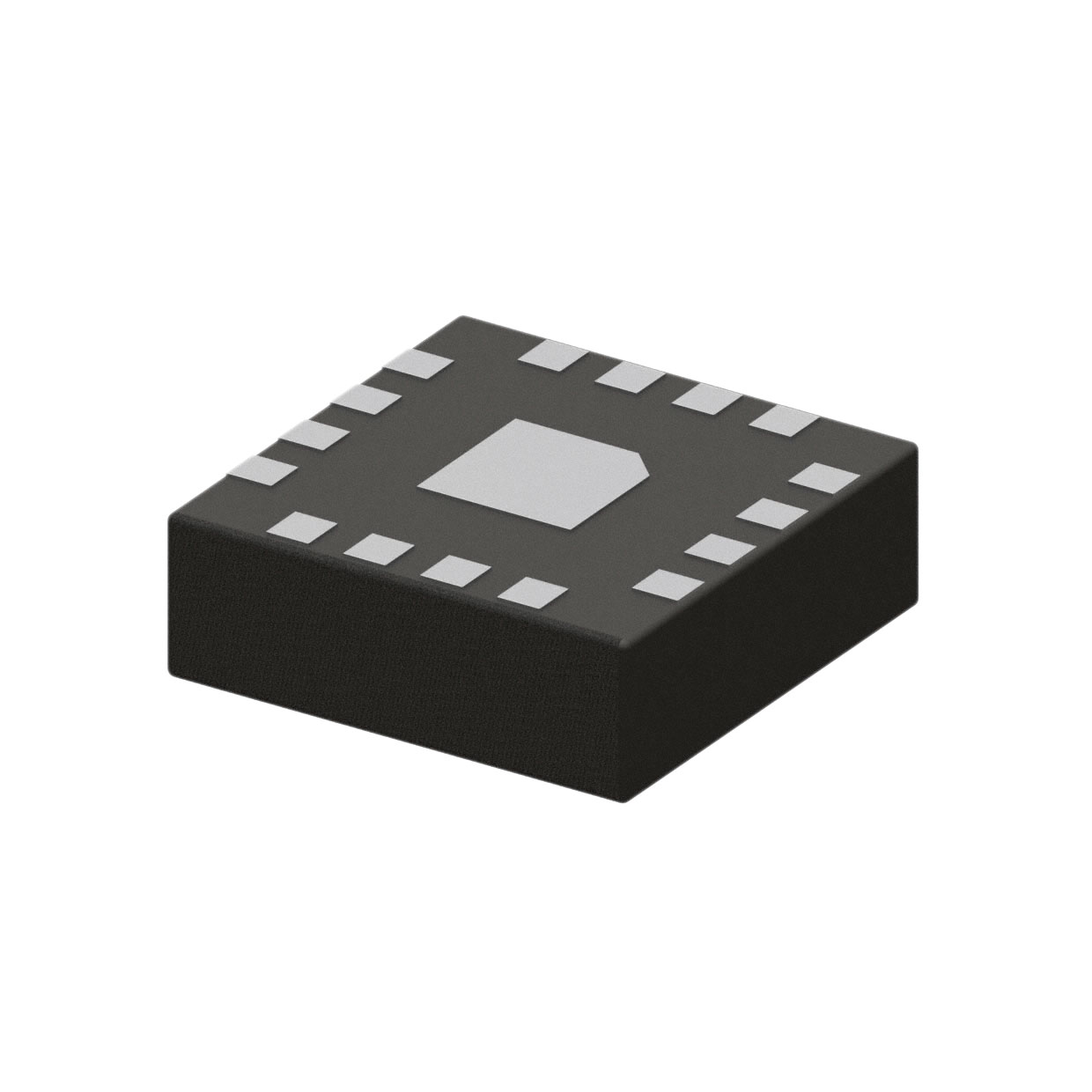
The 9FGV1005A000LTGI8 is a factory-configured programmable clock generator from Renesas Electronics' PhiClock family. It provides two output pairs with one integer-related frequency and one spread-spectrum or fractional frequency per configuration, plus two crystal reference copies. The device supports LP-HCSL and LVDS differential signaling standards with supply voltages of 1.8V and 3.3V. It operates within a temperature range of -40°C to 85°C and utilizes a 24-lead LGA package measuring 4.0 x 4.0 mm.
This component is a factory-configured device, meaning specific electrical parameters are determined at the time of manufacturing based on customer specifications. Verification should focus on confirming the exact output frequencies and configurations match the design requirements, as generic datasheets do not define these unique values. Ensure the package type and voltage levels align with the target system constraints before procurement.
Select this model when a dual-output clock generator with mixed integer and spread-spectrum capabilities is required for PCIe or similar high-speed serial links. Verify that the 1.8V and 3.3V supply rails are available in the target design. Consider the 24-lead LGA package dimensions (4.0 x 4.0 mm) for PCB layout compatibility. Confirm that the factory configuration process can accommodate the specific frequency plan needed for the application.
The 9FGV1005A000LTGI8 belongs to the 9FGV1005C series within the PhiClock family. This series is designed for applications requiring flexible clock generation with support for multiple output standards. The 'A' suffix typically denotes a specific factory configuration variant within the broader 9FGV1005 product line, sharing common architectural features with other members like the 9FGV1004 and 9FGV1006.
Direct replacements within the same family include the 9FGV1004CQ501LTGI8 and 9FGV1006Q550LTGI8, though pinouts and output configurations may differ. Verify that any substitute part supports the required LP-HCSL or LVDS outputs and matches the 1.8V/3.3V supply requirements. Cross-model substitution requires careful review of the specific factory configuration data.
 9FGV1005A000LTGI8
The activity of extra discounts on wholesale prices is in full swing…
Please fill in your contact information and we will send you the latest wholesale price list.