 ChipApex | Global Electronic Components Supplier
ADF4360-9BCPZRL
Search Product
Search Post
— IC芯片 | 连接器 | 传感器 | 被动器件 —
Search productSearch post
— IC芯片 | 连接器 | 传感器 | 被动器件 —
Consult the customer manager about the wholesale price.
consultation hotline:86-132-6715-2157
email:[email protected]
Contact the product manager for consultation. One-stop consultation is available.
Do you want a lower wholesale price? Please send us your inquiry and we will reply immediately.
The ADF4360-9BCPZRL is an integrated integer-N frequency synthesizer and voltage-controlled oscillator (VCO) manufactured by Analog Devices Inc. It operates within a primary output frequency range of 65 MHz to 400 MHz, determined by external inductors connected to pins L1 and L2. The device supports a 3-wire serial interface for register control and includes a programmable auxiliary divider stage that outputs frequencies from 1.1 MHz to 200 MHz. It functions on a single power supply ranging from 3.0 V to 3.6 V with 1.8 V logic compatibility. Key electrical specifications include a typical phase noise of -91 dBc/Hz at a 10 kHz offset and a lock time of approximately 400 µs.
Verify the specific suffix BCPZRL against the manufacturer's current ordering guide to confirm package type and tape/reel configuration. Ensure the component meets RoHS compliance requirements for the intended market. Confirm availability through authorized distributors as stock levels fluctuate.
Select external inductors carefully to set the desired VCO center frequency, noting that L1 and L2 must have identical values. Use a 470 Ω resistor in parallel with the inductors for standard operation. For low-frequency applications requiring reduced tuning voltage variation over temperature, consider increasing the VCO core power to 7.5 mA and using 240 Ω resistors instead of the default 470 Ω.
This component belongs to the ADF4360 family of frequency synthesizers. The ADF4360-9 variant is specifically optimized for lower frequency ranges (up to 400 MHz) compared to other family members that cover higher bands. It shares architectural similarities with other ADI PLL/VCO solutions but is distinct in its external inductor-dependent frequency setting mechanism.
Direct replacements within the same family include the ADF4360-0, ADF4360-1, ADF4360-4, ADF4360-5, ADF4360-7, and ADF4360-8. These variants differ primarily in their internal VCO frequency ranges. Verify that the replacement part covers the required 65 MHz to 400 MHz output spectrum before substitution.
The output frequency is set by the value of external inductors connected to pins L1 and L2. The datasheet specifies that L1 and L2 must be equal, and a 470 Ω resistor should be placed in parallel with them to AGND.
The DIVOUT pin provides access to the VCO signal divided by an integer A (ranging from 2 to 31) or divided by 2A. It can also be configured to output scaled versions of the reference frequency or N counter output.
Yes, the device supports 1.8 V logic compatibility, but the absolute maximum ratings and specifications indicate it can operate with DVDD up to 3.6 V, allowing for 3.3 V logic interfacing provided the input voltages remain within the specified VINH and VINL limits.
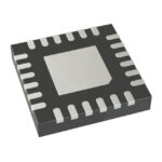 ADF4360-9BCPZRL
The activity of extra discounts on wholesale prices is in full swing…
Please fill in your contact information and we will send you the latest wholesale price list.





