 ChipApex | Global Electronic Components Supplier

SEARCH
Search Product
Search Post
— IC芯片 | 连接器 | 传感器 | 被动器件 —
Search productSearch post
— IC芯片 | 连接器 | 传感器 | 被动器件 —
Consult the customer manager about the wholesale price.
consultation hotline:86-132-6715-2157
email:[email protected]
Contact the product manager for consultation. One-stop consultation is available.
Do you want a lower wholesale price? Please send us your inquiry and we will reply immediately.
The AO4566 is a surface-mount N-channel Power MOSFET manufactured by Alpha & Omega Semiconductor Inc. It utilizes the latest Trench Power AlphaMOS (αMOS LV) technology to achieve very low on-resistance at a gate voltage of 4.5V and low gate charge. The device supports a drain-source voltage of 30V and a continuous drain current of 12A at Vgs=10V. Its maximum on-resistance is less than 11mΩ at Vgs=10V and less than 17mΩ at Vgs=4.5V. The component is RoHS and halogen-free compliant and has undergone 100% UIS and Rg testing.
Verify the specific manufacturer source, as the AO4566 designation appears in documentation from multiple entities including Alpha & Omega Semiconductor and Guangdong Kexin Industrial. Confirm that the datasheet corresponds to the intended electrical specifications, particularly the 30V rating and 12A current capability. Ensure compliance with RoHS and halogen-free requirements if mandated by the design. Check for any ordering suffixes that may indicate package variations or environmental certifications distinct from the standard product.
Select this component for designs requiring efficient power conversion at low gate drive voltages. The αMOS LV technology makes it suitable for logic-level driving scenarios where minimizing conduction losses is critical. The 30V rating provides adequate headroom for 24V or 12V bus systems. Consider the thermal management requirements associated with the TO-252 package when designing for high-current loads up to 12A. The 100% UIS testing ensures robustness against inductive load transients common in server and telecom environments.
The AO4566 belongs to the AlphaMOS family of N-channel enhancement mode field effect transistors. It is part of a series designed for general-purpose power switching applications. Similar devices in the market include the AO4568 and AO4490, which share comparable voltage ratings but differ in current handling and resistance specifications. The component is widely used in modern electronics where size efficiency and thermal performance are prioritized.
The maximum on-resistance (RDS(on)) at a gate-to-source voltage of 4.5V is less than 17mΩ.
Yes, the device undergoes 100% Unclamped Inductive Switching (UIS) testing to ensure reliability under inductive load conditions.
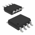 AO4566

The activity of extra discounts on wholesale prices is in full swing…
Please fill in your contact information and we will send you the latest wholesale price list.





