 ChipApex | Global Electronic Components Supplier

SEARCH
Search Product
Search Post
— IC芯片 | 连接器 | 传感器 | 被动器件 —
Search productSearch post
— IC芯片 | 连接器 | 传感器 | 被动器件 —
Consult the customer manager about the wholesale price.
consultation hotline:86-132-6715-2157
email:[email protected]
Contact the product manager for consultation. One-stop consultation is available.
Do you want a lower wholesale price? Please send us your inquiry and we will reply immediately.
The AO4840E is a dual N-channel enhancement mode field effect transistor from Alpha & Omega Semiconductor. It utilizes advanced trench technology to achieve low on-resistance and gate charge. The device features a drain-source voltage of 40V and a continuous drain current of 6A at VGS=10V. On-resistance is less than 28mΩ at VGS=10V and less than 35mΩ at VGS=4.5V. It includes typical ESD protection rated at HBM Class 2. The component is available in an SO-8 tape and reel package with a minimum order quantity of 3000 units.
Verify the specific ordering suffix against official manufacturer documentation before procurement. Confirm that the selected variant matches the required package type and form factor. Ensure compliance with applicable export control regulations and legal requirements during acquisition. Evaluate product suitability for intended applications independently.
Select this component based on its 40V rating and 6A continuous current capacity. Consider the thermal resistance characteristics when designing heat dissipation strategies. Verify that the gate threshold voltage meets the logic level requirements of the driving circuit. Check the maximum junction temperature limits for the operating environment.
This part belongs to the AlphaMOS series of dual N-channel MOSFETs. It shares the SO-8 surface mount package format with other devices in the family. The component is designed for general-purpose switching applications requiring moderate current handling capabilities.
Publicly confirmed substitute part numbers are not provided in the verified source material. Consult official manufacturer documentation for potential cross-references or alternative components.
The junction and storage temperature range is -55°C to 150°C.
Yes, the datasheet specifies that the device is 100% UIS tested.
The device offers typical ESD protection rated at HBM Class 2.
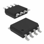 AO4840E

The activity of extra discounts on wholesale prices is in full swing…
Please fill in your contact information and we will send you the latest wholesale price list.





