 ChipApex | Global Electronic Components Supplier
SEARCH
Search Product
Search Post
— IC芯片 | 连接器 | 传感器 | 被动器件 —
Search productSearch post
— IC芯片 | 连接器 | 传感器 | 被动器件 —
Consult the customer manager about the wholesale price.
consultation hotline:86-132-6715-2157
email:[email protected]
Contact the product manager for consultation. One-stop consultation is available.
Do you want a lower wholesale price? Please send us your inquiry and we will reply immediately.
The AO6801E is a dual P-channel enhancement mode field effect transistor manufactured by Alpha & Omega Semiconductor. It utilizes advanced trench technology to deliver low on-resistance and minimal gate charge, making it suitable for load switch and PWM applications. The device features a drain-source voltage of -30V and a continuous drain current of -2.3A at VGS = -10V. On-resistance values are specified as less than 135mΩ at VGS = -10V, less than 185mΩ at VGS = -4.5V, and less than 265mΩ at VGS = -2.5V. It operates within a junction temperature range of -55°C to 150°C.
Verify the specific suffix 'E' against official manufacturer documentation to confirm if it denotes a specific tape and reel packaging variant or environmental compliance status distinct from the standard AO6801. Ensure the component matches the RoHS and Sony 259 specifications required for your assembly process.
Select this component when a compact dual P-channel solution is required for low-voltage switching. The low gate charge supports efficient PWM operation. Verify that the -30V rating and -2.3A current capacity align with the circuit's maximum operating conditions and thermal requirements.
This part belongs to the AO6801 series of dual P-channel MOSFETs. The base model AO6801 is electrically identical to the AO6801L green product option. The AO6801E likely represents a specific packaging or compliance variation within this family, sharing the same core electrical characteristics defined by the manufacturer's trench technology design.
AO6801
Yes, the standard AO6801 series meets RoHS and Sony 259 specifications for lead-free construction.
The datasheet specifies a maximum gate-source voltage (VGS) rating of ±12V.
RDS(ON) increases as gate voltage decreases: <135mΩ at -10V, <185mΩ at -4.5V, and <265mΩ at -2.5V.
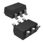 AO6801E
The activity of extra discounts on wholesale prices is in full swing…
Please fill in your contact information and we will send you the latest wholesale price list.





