 ChipApex | Global Electronic Components Supplier
SEARCH
Search Product
Search Post
— IC芯片 | 连接器 | 传感器 | 被动器件 —
Search productSearch post
— IC芯片 | 连接器 | 传感器 | 被动器件 —
Consult the customer manager about the wholesale price.
consultation hotline:86-132-6715-2157
email:[email protected]
Contact the product manager for consultation. One-stop consultation is available.
Do you want a lower wholesale price? Please send us your inquiry and we will reply immediately.
The AOB2618L is a surface-mount N-channel MOSFET from Alpha & Omega Semiconductor, utilizing trench technology for optimized high-frequency switching. It features a drain-source voltage of 60V and a continuous drain current of 23A at TC=25°C. The device offers an on-resistance of less than 19mΩ at VGS=10V and 25mΩ at VGS=4.5V. Key electrical parameters include a gate threshold voltage of 1.4V to 2.5V, total gate charge of 14nC to 20nC at 10V, and input capacitance of 950pF. It operates within a junction temperature range of -55°C to 175°C.
Verify the specific package variant required, as the datasheet covers multiple packages including TO-263 (D2PAK), TO-220, and TO-220F. Confirm that the application environment aligns with the consumer market qualification stated in the documentation. Ensure thermal management design accounts for the specified junction-to-case resistance values provided in the datasheet tables.
Select this component when a 60V rating is sufficient and low on-resistance is critical for efficiency. Compare the 23A continuous current limit against peak load requirements. Consider the TO-263 package for surface mount assembly needs. Evaluate the gate charge specifications against driver capabilities to ensure adequate switching speed without excessive drive current demands.
The AOB2618L belongs to the AOT2618L/AOB2618L/AOTF2618L family, sharing identical electrical characteristics but differing in physical packaging. It is part of Alpha & Omega Semiconductor's trench MOSFET lineup designed for general-purpose power switching. The 'L' suffix typically denotes lead-free compliance, consistent with RoHS standards mentioned in related product descriptions.
Electrically equivalent parts include AOT2618L and AOTF2618L. These share the same datasheet specifications but utilize different packages: TO-220 and TO-220F respectively. Verify pinout compatibility and thermal pad configuration before substituting, as package dimensions differ significantly between D2PAK and axial leads.
The maximum junction temperature is 175°C, as specified in the absolute maximum ratings and thermal characteristic notes.
Yes, the device undergoes 100% UIS testing, and single-pulse avalanche capability data is provided in the typical electrical characteristics.
The on-resistance is less than 19mΩ at VGS=10V and increases to less than 25mΩ at VGS=4.5V, allowing for logic-level driving considerations.
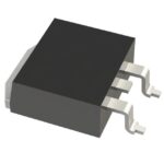 AOB2618L
The activity of extra discounts on wholesale prices is in full swing…
Please fill in your contact information and we will send you the latest wholesale price list.





