 ChipApex | Global Electronic Components Supplier

SEARCH
Search Product
Search Post
— IC芯片 | 连接器 | 传感器 | 被动器件 —
Search productSearch post
— IC芯片 | 连接器 | 传感器 | 被动器件 —
Consult the customer manager about the wholesale price.
consultation hotline:86-132-6715-2157
email:[email protected]
Contact the product manager for consultation. One-stop consultation is available.
Do you want a lower wholesale price? Please send us your inquiry and we will reply immediately.
The AOD32324 is an N-channel Power MOSFET from Alpha & Omega Semiconductor, housed in a TO-252 (DPAK) surface-mount package. It features a drain-source voltage (Vdss) of 30 V and continuous drain current ratings of 33 A at ambient temperature (Ta) and 70 A at case temperature (Tc). The device exhibits a maximum on-resistance (Rds(on)) of 3.4 mΩ at Vgs = 10 V and Id = 69 A. Gate threshold voltage (Vgs(th)) is typically 2.3 V at Id = 250 µA. Total gate charge (Qg) is 53.5 nC at Vgs = 10 V. Input capacitance (Ciss) is 400 pF at Vds = 20 V. Maximum power dissipation is 6.2 W at Ta and 69 W at Tc. Operating junction temperature range is -55°C to 175°C.
Verify the specific suffix code against the manufacturer's official datasheet to confirm exact electrical tolerances and packaging variations. Ensure the component source is an authorized distributor to guarantee authenticity and traceability. Cross-reference the date code and lot number with the supplier's certificate of conformity. Confirm that the storage and handling conditions meet ESD protection standards during procurement and assembly processes.
Select this component when a 30 V rating and high continuous current capacity are required in a TO-252 package. Evaluate the thermal resistance parameters relative to the PCB copper area to ensure adequate heat dissipation for the intended power dissipation levels. Compare the gate charge specifications against the driving circuit capabilities to optimize switching speed and minimize switching losses in the target application design.
Alpha & Omega Semiconductor specializes in discrete power devices and wide bandgap solutions. The AOD32324 belongs to their portfolio of high-performance MOSFETs designed for advanced electronics. These components support applications requiring efficient power management, including data centers, automotive electronics, and industrial motor controls, leveraging integrated process technology and advanced packaging know-how.
Check for direct substitutes within the same 30 V N-channel DPAK family from Alpha & Omega Semiconductor. Verify pinout compatibility and thermal pad configuration before substitution. Ensure replacement parts meet or exceed the original Rds(on), Vdss, and current ratings. Consult official cross-reference lists for validated alternatives.
The maximum drain-source voltage (Vdss) is 30 V.
It is available in a TO-252 (DPAK) surface-mount package.
The gate threshold voltage (Vgs(th)) is typically 2.3 V at a drain current of 250 µA.
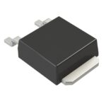 AOD32324

The activity of extra discounts on wholesale prices is in full swing…
Please fill in your contact information and we will send you the latest wholesale price list.





