 ChipApex | Global Electronic Components Supplier

SEARCH
Search Product
Search Post
— IC芯片 | 连接器 | 传感器 | 被动器件 —
Search productSearch post
— IC芯片 | 连接器 | 传感器 | 被动器件 —
Consult the customer manager about the wholesale price.
consultation hotline:86-132-6715-2157
email:[email protected]
Contact the product manager for consultation. One-stop consultation is available.
Do you want a lower wholesale price? Please send us your inquiry and we will reply immediately.
The AOD409G is a P-Channel Enhancement Mode Field Effect Transistor manufactured by Alpha & Omega Semiconductor. It utilizes advanced trench power MOSFET technology to achieve low on-resistance and logic-level driving capabilities. The device features a Drain-Source Voltage (VDS) of -60V, a continuous drain current (ID) of -28A at VGS=-10V, and a maximum pulsed drain current (IDM) of -80A. Static drain-source on-resistance (RDS(ON)) is less than 40mΩ at VGS=-10V and less than 55mΩ at VGS=-4.5V. The component is housed in a TO-252 package with a junction temperature range of -55°C to 150°C.
Verify the specific ordering suffix 'G' corresponds to the Tape & Reel form factor containing 2500 units per reel as documented in the official datasheet. Confirm that the procurement specification aligns with the TO-252 package type and the electrical parameters listed for the AOD409G variant. Ensure compliance requirements match the RoHS and Halogen-Free status indicated in the product summary.
Select this component when designing circuits requiring a -60V P-Channel MOSFET with high current handling up to -28A. The low RDS(ON) values at both -10V and -4.5V gate voltages make it suitable for logic-level interface applications. Consider the thermal characteristics, specifically the junction-to-case resistance of 2.1°C/W, for adequate heatsinking in motor drive or industrial environments where power dissipation management is critical.
The AOD409G belongs to the AOD409 series of P-Channel MOSFETs produced by Alpha & Omega Semiconductor. This series employs trench technology to deliver enhanced performance metrics compared to standard planar devices. The G suffix typically denotes the tape and reel packaging configuration, distinguishing it from other potential packaging options within the same electrical family.
Direct replacement requires verifying pinout compatibility (Gate, Source, Drain) and ensuring the substitute part meets or exceeds the -60V voltage rating and -28A current capacity. Check that the replacement device supports the required logic-level gate drive thresholds and operates within the specified -55°C to 150°C junction temperature range.
The maximum pulsed drain current (IDM) is -80A.
Yes, the datasheet specifies that the device undergoes 100% Unclamped Inductive Switching (UIS) testing.
The gate threshold voltage (VGS(th)) ranges from -1.5V to -2.5V under standard test conditions.
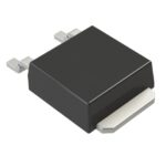 AOD409G

The activity of extra discounts on wholesale prices is in full swing…
Please fill in your contact information and we will send you the latest wholesale price list.





