 ChipApex | Global Electronic Components Supplier

SEARCH
Search Product
Search Post
— IC芯片 | 连接器 | 传感器 | 被动器件 —
Search productSearch post
— IC芯片 | 连接器 | 传感器 | 被动器件 —
Consult the customer manager about the wholesale price.
consultation hotline:86-132-6715-2157
email:[email protected]
Contact the product manager for consultation. One-stop consultation is available.
Do you want a lower wholesale price? Please send us your inquiry and we will reply immediately.
The AOD413A is a P-Channel Enhancement Mode Field Effect Transistor manufactured by Alpha & Omega Semiconductor. It utilizes advanced trench technology to achieve low on-resistance and gate charge. The device features a Drain-Source Voltage (VDS) of -40V and a Continuous Drain Current (ID) of -12A at VGS = -10V. The maximum On-State Resistance (RDS(ON)) is less than 44mΩ at VGS = -10V and less than 66mΩ at VGS = -4.5V. It is housed in a TO-252 (DPAK) package with a Maximum Junction Temperature of 175°C.
Verify the component datasheet revision and manufacturing date code against the latest official Alpha & Omega Semiconductor documentation. Confirm that the specific unit received matches the TO-252 (DPAK) package outline and pin configuration. Ensure compliance with consumer market qualification standards as defined by the manufacturer.
Select this component for designs requiring a -40V P-Channel MOSFET with a continuous drain current rating of -12A. Consider the thermal resistance characteristics of the DPAK package when determining heatsinking requirements. Verify that the gate drive voltage meets the threshold for the required on-resistance specifications.
The AOD413A belongs to the family of P-Channel Enhancement Mode Field Effect Transistors produced by Alpha & Omega Semiconductor. It is designed using trench technology to optimize conduction losses and switching efficiency within a surface-mountable TO-252 (DPAK) footprint.
No public confirmed substitute part numbers are available in the provided source material.
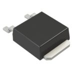 AOD413A

The activity of extra discounts on wholesale prices is in full swing…
Please fill in your contact information and we will send you the latest wholesale price list.





