 ChipApex | Global Electronic Components Supplier

SEARCH
Search Product
Search Post
— IC芯片 | 连接器 | 传感器 | 被动器件 —
Search productSearch post
— IC芯片 | 连接器 | 传感器 | 被动器件 —
Consult the customer manager about the wholesale price.
consultation hotline:86-132-6715-2157
email:[email protected]
Contact the product manager for consultation. One-stop consultation is available.
Do you want a lower wholesale price? Please send us your inquiry and we will reply immediately.
The AOD4186 is a 40V N-Channel MOSFET manufactured by Alpha & Omega Semiconductor Inc. It utilizes advanced trench technology to achieve extremely low on-resistance, making it suitable for low voltage inverter applications. The device features a TO-252 (D-Pak) package with an absolute maximum drain-source voltage of 40V and a gate-source voltage rating of ±20V. At VGS=10V, the maximum on-resistance is 15mΩ, while at VGS=4.5V, it is 19mΩ. The continuous drain current reaches 35A at TC=25°C and 27A at TA=70°C. The junction temperature range spans from -55°C to 175°C.
Verify component authenticity through authorized distribution channels. Confirm datasheet revision status matches design requirements. Ensure packaging specifications align with assembly line capabilities. Validate compliance with applicable export control regulations and RoHS standards prior to integration into final products.
Evaluate thermal performance based on specific board copper area and ambient conditions. Consider derating curves for continuous operation above 25°C case temperature. Verify gate drive voltage compatibility with the specified RDS(ON) thresholds. Assess avalanche energy ratings if used in inductive load environments.
This component belongs to the AOS D-Pak series of power MOSFETs designed for surface mount applications. It shares the industry-standard TO-252 footprint common in various power electronics designs. The device represents a balance between current handling capability and thermal dissipation for compact circuit layouts.
Cross-reference pinout configurations and thermal resistance values when substituting. Verify that alternative devices meet or exceed the 40V breakdown voltage and 15mΩ on-resistance specifications. Check package dimensions for mechanical fitment compatibility.
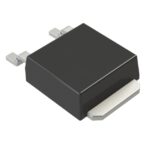 AOD4186

The activity of extra discounts on wholesale prices is in full swing…
Please fill in your contact information and we will send you the latest wholesale price list.





