ChipApex | Global Electronic Components Supplier

SEARCH
Search Product
Search Post
— IC芯片 | 连接器 | 传感器 | 被动器件 —
Search productSearch post
— IC芯片 | 连接器 | 传感器 | 被动器件 —
Consult the customer manager about the wholesale price.
consultation hotline:86-132-6715-2157
email:[email protected]
Contact the product manager for consultation. One-stop consultation is available.
Do you want a lower wholesale price? Please send us your inquiry and we will reply immediately.
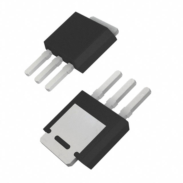
The AOI442 is a 60V N-Channel Enhancement Mode Field Effect Transistor manufactured by Alpha & Omega Semiconductor Inc. It utilizes advanced trench technology to achieve low on-resistance and gate charge, making it suitable for load switch and PWM applications. The device is housed in a TO-252 (DPAK) package. Key electrical parameters include a drain-source breakdown voltage of 60V, a continuous drain current of 37A at VGS=10V, and a maximum on-resistance of less than 20mΩ at VGS=10V and 25mΩ at VGS=4.5V.
Verify the specific ordering suffix against the manufacturer's official documentation to ensure correct packaging and environmental compliance specifications. Confirm that the component meets RoHS standards if required by your design constraints. Cross-reference the datasheet revision date to ensure alignment with the latest thermal and electrical characteristic updates provided by Alpha & Omega Semiconductor.
Select this component for designs requiring a 60V N-channel MOSFET with high current capability in a surface-mount DPAK package. Consider the thermal resistance values when designing heat dissipation strategies, as power dissipation limits are dependent on the case temperature and board copper area. Ensure the gate drive voltage supports the specified RDS(ON) thresholds for optimal efficiency.
The AOI442 belongs to the AOD442/AOI442 family of 60V N-Channel MOSFETs from Alpha & Omega Semiconductor. These devices are engineered for general-purpose power switching applications where low conduction losses and fast switching speeds are critical. The 'I' suffix typically denotes a specific tape and reel packaging option compared to the standard bulk or alternative packaging of the base AOD442 model.
Direct substitutes must match the 60V rating, N-channel configuration, and TO-252 package. Verify pinout compatibility and ensure equivalent or superior RDS(ON) and Qg specifications. Check for identical thermal impedance characteristics to maintain existing cooling solutions without modification.
Yes, the datasheet specifies that the device undergoes 100% Unclamped Inductive Switching (UIS) testing to verify its ruggedness and avalanche capability.
The maximum junction temperature range is -55°C to 175°C.
 AOI442

The activity of extra discounts on wholesale prices is in full swing…
Please fill in your contact information and we will send you the latest wholesale price list.