ChipApex | Global Electronic Components Supplier

SEARCH
Search Product
Search Post
— IC芯片 | 连接器 | 传感器 | 被动器件 —
Search productSearch post
— IC芯片 | 连接器 | 传感器 | 被动器件 —
Consult the customer manager about the wholesale price.
consultation hotline:86-132-6715-2157
email:[email protected]
Contact the product manager for consultation. One-stop consultation is available.
Do you want a lower wholesale price? Please send us your inquiry and we will reply immediately.
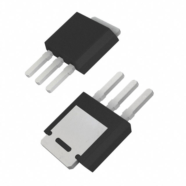
AOI468 is listed in the Single FETs, MOSFETs range at ChipApex. The manufacturer field lists Alpha & Omega Semiconductor Inc.. Its product description is MOSFET N CH 300V 11.5A TO252. Review the specifications below when checking this part for your BOM.
The AOI468 is a 300V N-Channel MOSFET fabricated using an advanced high voltage process. It features a maximum continuous drain current of 11.5A at VGS=10V and a typical on-resistance (RDS(ON)) of 0.31Ω at VGS=10V, with a maximum of 0.42Ω. The device supports a pulsed drain current of 29A and has a gate threshold voltage ranging from 3.4V to 4.5V. Key dynamic parameters include a total gate charge of 12.8nC typical and input capacitance of 632pF typical. It operates within a junction temperature range of -50°C to 175°C.
Verify the specific suffix or package variant required, as datasheets often list multiple part numbers (e.g., AOD468 vs AOI468) which may differ in packaging or thermal characteristics. Confirm RoHS compliance status and lead time availability directly with Alpha & Omega Semiconductor or authorized distributors, as stock levels fluctuate. Ensure the selected component meets the specific thermal management requirements for the target application environment.
Select this component for applications requiring 300V blocking capability and moderate current handling up to 11.5A. Consider the thermal resistance values (RθJA and RθJC) when designing heatsinking solutions. Verify that the gate drive voltage can reliably exceed the 4.5V maximum threshold to ensure full enhancement. Evaluate the single-pulse avalanche energy limits if the circuit is prone to inductive load switching transients.
The AOI468 belongs to the AOS high-voltage MOSFET family designed for AC-DC conversion. It shares design similarities with the AOD468 but typically differs in packaging or specific thermal ratings. These devices are engineered to replace older generation MOSFETs in offline power supplies, offering better performance through lower on-resistance and optimized capacitive characteristics for faster switching speeds.
Check pinout compatibility with existing TO-252 or TO-251A footprints. Compare RDS(ON) and Qg values against current components to ensure equivalent or improved efficiency. Verify that the replacement part's breakdown voltage and current ratings meet or exceed the original design specifications.
Yes, the datasheet explicitly states that the device is 100% UIS (Unclamped Inductive Switching) tested and guarantees avalanche capability.
The maximum junction temperature (TJ) and storage temperature range is specified as -50°C to 175°C.
Explore related parts through FETs, MOSFETs, Transistors, Discrete Semiconductor Products, all product categories.
 AOI468

The activity of extra discounts on wholesale prices is in full swing…
Please fill in your contact information and we will send you the latest wholesale price list.