ChipApex | Global Electronic Components Supplier

SEARCH
Search Product
Search Post
— IC芯片 | 连接器 | 传感器 | 被动器件 —
Search productSearch post
— IC芯片 | 连接器 | 传感器 | 被动器件 —
Consult the customer manager about the wholesale price.
consultation hotline:86-132-6715-2157
email:[email protected]
Contact the product manager for consultation. One-stop consultation is available.
Do you want a lower wholesale price? Please send us your inquiry and we will reply immediately.
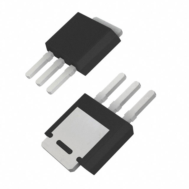
The AOI510 is a 30V N-Channel AlphaMOS power transistor designed for high-efficiency switching applications. It features an on-resistance of less than 2.6mΩ at VGS=10V and less than 4mΩ at VGS=4.5V, ensuring low conduction losses. The device supports a continuous drain current of 70A at TA=25°C and withstands a gate-source voltage of ±20V. With a maximum junction temperature range of -55°C to 175°C and 100% UIS testing, it provides robust performance in demanding environments.
Verify the specific package variant required, as the datasheet covers multiple form factors including TO-251A, IPAK, and TO-252. Confirm that the component meets RoHS and Halogen-Free compliance standards if mandated by your assembly process. Ensure the design accounts for the specified thermal resistance values relative to the chosen PCB copper area and mounting conditions.
Select this component when low conduction loss at standard logic-level gate voltages is critical. The device is suitable for applications requiring high current density within a compact footprint. Consider the thermal management requirements based on the junction-to-case resistance provided in the datasheet. Verify that the operating voltage remains within the 30V breakdown limit under all transient conditions.
This part belongs to the AOD510/AOI510 series from Alpha & Omega Semiconductor Inc., utilizing their proprietary αMOS LV trench technology. It is engineered primarily for consumer market applications but offers reliability suitable for industrial and telecom sectors. The product line emphasizes high current capability and low on-resistance to improve overall system efficiency in power conversion circuits.
Check pinout compatibility if substituting with other 30V N-channel MOSFETs in DPAK or similar packages. Ensure the replacement device meets or exceeds the 70A continuous current rating and the <4mΩ RDS(on) specification at 4.5V VGS to maintain circuit performance.
The absolute maximum gate-source voltage is ±20V.
Yes, the datasheet confirms 100% UIS testing has been performed.
The typical total gate charge (Qg) at VGS=10V is 44nC, with a maximum of 60nC.
 AOI510

The activity of extra discounts on wholesale prices is in full swing…
Please fill in your contact information and we will send you the latest wholesale price list.