 ChipApex | Global Electronic Components Supplier
SEARCH
Search Product
Search Post
— IC芯片 | 连接器 | 传感器 | 被动器件 —
Search productSearch post
— IC芯片 | 连接器 | 传感器 | 被动器件 —
Consult the customer manager about the wholesale price.
consultation hotline:86-132-6715-2157
email:[email protected]
Contact the product manager for consultation. One-stop consultation is available.
Do you want a lower wholesale price? Please send us your inquiry and we will reply immediately.
The AON3814 is a dual N-channel enhancement mode field effect transistor manufactured by Alpha & Omega Semiconductor Inc. It utilizes advanced trench technology to achieve low on-resistance and gate charge, supporting operation with gate voltages as low as 1.8V while maintaining a maximum VGS rating of ±12V. The device features a common-drain configuration suitable for load switch applications. Key electrical parameters include a drain-source voltage (BVDSS) of 20V, a continuous drain current (ID) of 6A at VGS=4.5V, and an on-state resistance (RDS(ON)) of less than 17mΩ at VGS=4.5V. The component is housed in a DFN 3x3 package.
Verify the specific datasheet revision and manufacturing lot details upon procurement. Confirm that the received components match the DFN 3x3 package dimensions and pinout configuration specified in the official Alpha & Omega Semiconductor documentation. Ensure compliance with RoHS standards if required by the end application.
Select this component for applications requiring a dual N-channel MOSFET in a compact DFN 3x3 footprint. Consider the 20V drain-source voltage and 6A continuous current ratings against the circuit requirements. Evaluate the low gate charge and threshold voltage capabilities for efficient drive circuits operating at low logic levels.
The AON3814 belongs to the family of dual N-channel MOSFETs produced by Alpha & Omega Semiconductor Inc. It shares the DFN 3x3 package form factor with other devices in the series but is distinguished by its specific 20V voltage rating and 6A current capability. The common-drain topology differentiates it from standard common-source configurations found in many power switching applications.
Publicly confirmed substitute part numbers are not available in the provided source material. Verify compatibility with existing designs by comparing absolute maximum ratings, thermal characteristics, and pinout assignments before substituting with alternative dual N-channel MOSFETs.
The maximum gate-source voltage (VGS) rating is ±12V.
The typical total gate charge (Qg) is 11 nC when measured at VGS=4.5V, VDS=10V, and ID=6A.
Yes, the device is explicitly described as ESD protected in the general description.
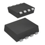 AON3814
The activity of extra discounts on wholesale prices is in full swing…
Please fill in your contact information and we will send you the latest wholesale price list.




