ChipApex | Global Electronic Components Supplier

SEARCH
Search Product
Search Post
— IC芯片 | 连接器 | 传感器 | 被动器件 —
Search productSearch post
— IC芯片 | 连接器 | 传感器 | 被动器件 —
Consult the customer manager about the wholesale price.
consultation hotline:86-132-6715-2157
email:[email protected]
Contact the product manager for consultation. One-stop consultation is available.
Do you want a lower wholesale price? Please send us your inquiry and we will reply immediately.
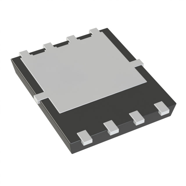
AON6482 is listed in the Single FETs, MOSFETs range at ChipApex. The manufacturer field lists Alpha & Omega Semiconductor Inc.. Its product description is MOSFET N-CH 100V 5.5A/28A 8DFN. Review the specifications below when checking this part for your BOM.
The AON6482 is a 100V N-Channel MOSFET utilizing advanced trench technology for low on-resistance. It features a maximum drain-source voltage of 100V and continuous drain current ratings of 28A at 25°C case temperature and 20A at 70°C case temperature. The device offers an on-resistance of less than 37mΩ at VGS=10V and less than 42mΩ at VGS=4.5V. It includes 100% UIS testing, operates within a junction temperature range of -55°C to 175°C, and utilizes an 8-pin DFN5x6 package.
Verify the specific revision status and datasheet version before procurement, as thermal parameters like RqJA depend on board design. Confirm that the application environment supports the specified junction temperature limits. Ensure compatibility with the 8-DFN package footprint during PCB layout. Review absolute maximum ratings carefully to prevent overstress during transient events.
Select this component when a 100V rating is required alongside high efficiency in synchronous rectification or boost topologies. The low gate charge and fast switching times make it suitable for high-frequency applications. Consider the thermal management requirements based on the junction-to-ambient resistance if heatsinking is not utilized. Verify that the gate drive voltage aligns with the optimal RDS(ON) performance ranges.
The AON6482 belongs to Alpha & Omega Semiconductor's portfolio of N-Channel MOSFETs designed for power management applications. It leverages trench technology to achieve superior conduction losses compared to standard planar devices. The device is packaged in a compact DFN5x6 form factor, facilitating surface-mount assembly in space-constrained designs common in modern electronic equipment.
Public confirmed substitute part numbers are not available in the provided documentation. Consult manufacturer cross-reference guides for potential alternatives with matching voltage, current, and package specifications.
Yes, the device has undergone 100% Unclamped Inductive Switching (UIS) testing to verify its capability to handle inductive load energy.
The maximum junction temperature (TJ) and storage temperature range for the AON6482 is -55°C to 175°C.
The on-resistance is specified as less than 37mΩ at VGS=10V and less than 42mΩ at VGS=4.5V, indicating improved conduction at higher gate drive voltages.
Explore related parts through FETs, MOSFETs, Transistors, Discrete Semiconductor Products, all product categories.
 AON6482

The activity of extra discounts on wholesale prices is in full swing…
Please fill in your contact information and we will send you the latest wholesale price list.