ChipApex | Global Electronic Components Supplier
SEARCH
Search Product
Search Post
— IC芯片 | 连接器 | 传感器 | 被动器件 —
Search productSearch post
— IC芯片 | 连接器 | 传感器 | 被动器件 —
Consult the customer manager about the wholesale price.
consultation hotline:86-132-6715-2157
email:[email protected]
Contact the product manager for consultation. One-stop consultation is available.
Do you want a lower wholesale price? Please send us your inquiry and we will reply immediately.
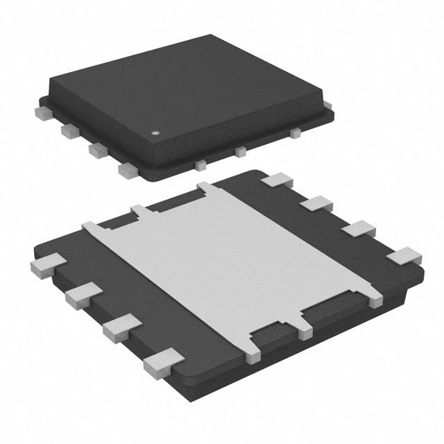
The AON6810 is a dual N-channel enhancement mode MOSFET array utilizing AlphaMOS trench technology. It features a 30V drain-source voltage and a continuous drain current of 20A at VGS=10V. The device offers very low on-resistance, specified as less than 4.4mΩ at VGS=10V and less than 6.5mΩ at VGS=4.5V. Total gate charge is typically 34nC at 10V and 20nC at 4.5V. Input capacitance is 1720pF at 15V. The component includes an integrated temperature sense diode and provides ESD protection rated at HBM Class 3A. It operates within a junction temperature range of -55°C to 150°C.
Verify the specific package marking and date code against the manufacturer's latest datasheet revision before integration. Confirm that the intended application environment remains within the consumer market scope, as critical life support uses are explicitly excluded from qualification. Ensure thermal design accounts for the specified junction-to-ambient resistance values under actual board copper constraints.
Select this component when a dual N-channel solution with a shared source terminal is required in a compact footprint. The low gate threshold and high current capability make it suitable for direct microcontroller driving. Evaluate the thermal performance based on the specific PCB copper area, as the junction-to-ambient resistance varies significantly with board layout dimensions.
This part belongs to the AlphaMOS LV series from Alpha & Omega Semiconductor Inc., designed for low-voltage power switching. It utilizes advanced trench technology to achieve superior conduction losses compared to standard planar devices. The dual common-drain architecture allows for efficient space utilization in portable electronics and battery-powered equipment requiring synchronized switching functions.
No public confirmed substitute part numbers are available in the provided documentation.
 AON6810
The activity of extra discounts on wholesale prices is in full swing…
Please fill in your contact information and we will send you the latest wholesale price list.