ChipApex | Global Electronic Components Supplier
SEARCH
Search Product
Search Post
— IC芯片 | 连接器 | 传感器 | 被动器件 —
Search productSearch post
— IC芯片 | 连接器 | 传感器 | 被动器件 —
Consult the customer manager about the wholesale price.
consultation hotline:86-132-6715-2157
email:[email protected]
Contact the product manager for consultation. One-stop consultation is available.
Do you want a lower wholesale price? Please send us your inquiry and we will reply immediately.
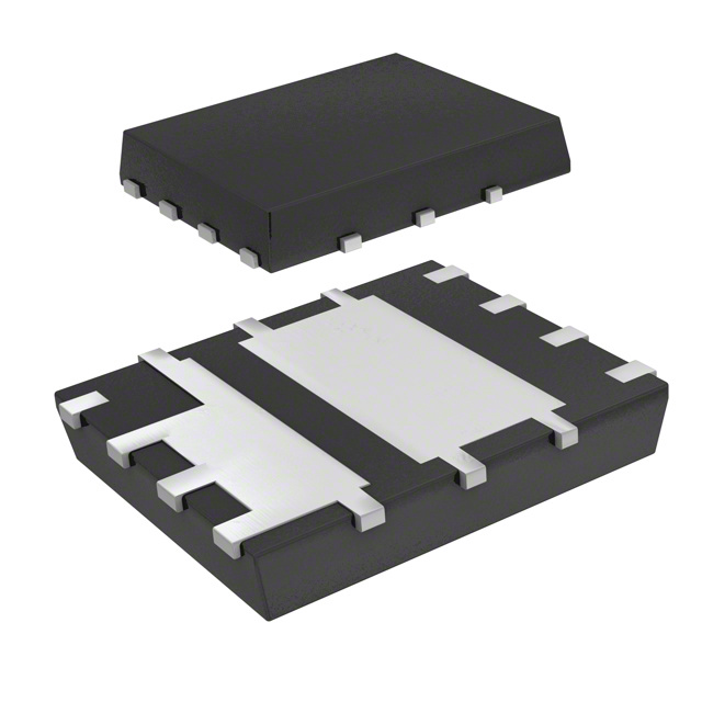
The AON6906A is a dual asymmetric N-channel MOSFET array in an 8-DFN (5x6) package. It integrates two specialized transistors for synchronous buck power stages: Q1 optimized for switching and Q2 for conduction. Key parameters include a Drain-Source Voltage of 30V, Gate-Source Voltage of ±20V, and a Junction Temperature range of -55°C to 150°C. Q1 features a maximum RDS(ON) of 14.4mΩ at VGS=10V/ID=9.1A and 21.3mΩ at VGS=4.5V/ID=9.1A, with a max gate charge of 9nC @ 10V. Q2 offers a lower RDS(ON) of 11.7mΩ at VGS=10V/ID=10A and 17.5mΩ at VGS=4.5V/ID=10A, with a max gate charge of 10nC @ 10V.
Verify component authenticity through authorized Alpha & Omega Semiconductor channels or certified distributors. Confirm the specific revision level matches design requirements. Ensure storage conditions adhere to moisture sensitivity guidelines prior to soldering. Validate that the intended operating environment remains within the specified thermal and electrical limits defined in the datasheet.
Select this component when board real estate is limited and distinct high-side and low-side performance profiles are required. The asymmetric nature allows designers to optimize switching speed independently from conduction efficiency. Verify that the 30V rating accommodates system voltage spikes and that the 8-DFN package thermal impedance suits the application's heat dissipation needs.
The AON6906A belongs to the AON6906 family of dual MOSFET arrays. It utilizes trench technology to achieve low on-resistance and fast switching speeds. This device represents a solution for modern power management applications requiring high density and efficiency in compact surface-mount packages.
Check for direct pin-compatible alternatives within the same manufacturer's portfolio that offer similar asymmetric configurations. Verify that any substitute maintains the 30V rating and comparable thermal resistance values to ensure circuit stability without redesign.
Q1 is optimized as the high-side switch to minimize switching losses, while Q2 is optimized as the low-side switch to provide lower on-resistance for reduced conduction losses.
Yes, the datasheet specifies that the device undergoes 100% Unclamped Inductive Switching (UIS) testing.
It features a "Schottky style" soft recovery body diode, which helps control switching behavior and minimize losses during diode recovery.
 AON6906A
The activity of extra discounts on wholesale prices is in full swing…
Please fill in your contact information and we will send you the latest wholesale price list.