ChipApex | Global Electronic Components Supplier
SEARCH
Search Product
Search Post
— IC芯片 | 连接器 | 传感器 | 被动器件 —
Search productSearch post
— IC芯片 | 连接器 | 传感器 | 被动器件 —
Consult the customer manager about the wholesale price.
consultation hotline:86-132-6715-2157
email:[email protected]
Contact the product manager for consultation. One-stop consultation is available.
Do you want a lower wholesale price? Please send us your inquiry and we will reply immediately.
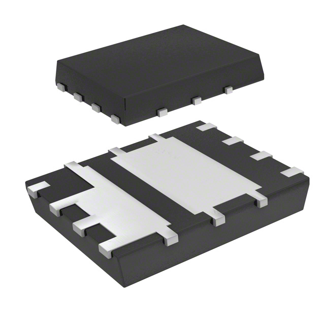
The AON6928 is a dual asymmetric N-channel MOSFET utilizing AlphaMOS LV technology, housed in a DFN5X6 package. It integrates two distinct channels with differing current and resistance capabilities. Channel Q1 provides a continuous drain current of 30A at VGS=10V with an on-resistance below 8.2mΩ. Channel Q2 delivers 36A at VGS=10V with an on-resistance under 2.9mΩ. Both channels maintain a 30V drain-source breakdown voltage. The device features low gate charge and high current capability, suitable for power switching applications.
Verify the specific ordering suffix and tape/reel quantity requirements directly with the manufacturer or authorized distributors before placing orders. Confirm that the component meets RoHS and Halogen-Free compliance standards required by your assembly process. Ensure the design accommodates the DFN5X6 package thermal constraints and soldering profiles specified in the datasheet.
Select this component when a dual asymmetric layout is required to optimize board space and performance for mixed-load scenarios. Consider the lower on-resistance of Q2 for higher current paths and Q1 for standard switching duties. Evaluate the thermal dissipation capabilities based on the specific PCB copper area and airflow conditions, as the junction-to-ambient resistance varies significantly with board design.
This component belongs to the Alpha & Omega Semiconductor dual MOSFET portfolio, specifically designed for low-voltage, high-current applications. It leverages the αMOS LV platform to enhance efficiency in modern power management systems where low gate drive voltages are prevalent. The DFN5X6 package offers a balance between thermal performance and footprint reduction compared to traditional leaded packages.
No direct public substitute part numbers are documented for the AON6928. Designers must evaluate alternative dual asymmetric MOSFETs from other manufacturers based on pin compatibility, electrical parameters, and thermal characteristics if substitution is necessary.
Channel Q2 is optimized for higher current handling (36A vs 30A) and lower on-resistance (<2.9mΩ vs <8.2mΩ) compared to Channel Q1, making it suitable for heavier loads while Q1 serves standard switching functions.
Yes, the device utilizes αMOS LV technology to achieve very low RDS(on) at a VGS of 4.5V, ensuring efficient operation with lower gate drive voltages.
The AON6928 is packaged in a DFN5X6 (5x6mm Dual Flat No-Lead) surface-mount package.
 AON6928
The activity of extra discounts on wholesale prices is in full swing…
Please fill in your contact information and we will send you the latest wholesale price list.