ChipApex | Global Electronic Components Supplier
SEARCH
Search Product
Search Post
— IC芯片 | 连接器 | 传感器 | 被动器件 —
Search productSearch post
— IC芯片 | 连接器 | 传感器 | 被动器件 —
Consult the customer manager about the wholesale price.
consultation hotline:86-132-6715-2157
email:[email protected]
Contact the product manager for consultation. One-stop consultation is available.
Do you want a lower wholesale price? Please send us your inquiry and we will reply immediately.
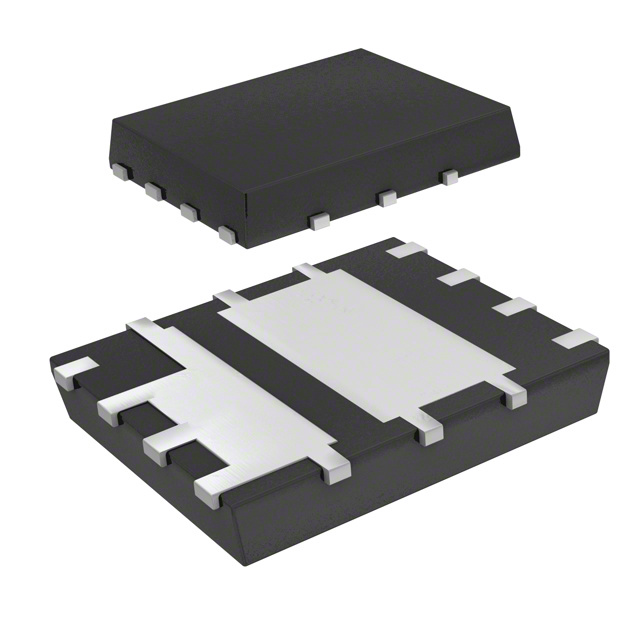
The AONY36306 is a dual asymmetric N-channel MOSFET manufactured by Alpha & Omega Semiconductor Inc. It utilizes Trench Power MOSFET technology and is housed in a DFN 5x6B package. The device features two distinct channels with different electrical characteristics. Q1 has a drain-source voltage (VDS) of 30V, continuous drain current (ID) of 32A at VGS=10V, and an on-resistance (RDS(ON)) of less than 6mΩ at VGS=10V and 8.6mΩ at VGS=4.5V. Q2 also has a VDS of 30V and ID of 32A, but offers lower on-resistance of less than 3.8mΩ at VGS=10V and 4.7mΩ at VGS=4.5V. Both channels are rated for a junction temperature range of -55°C to 150°C.
Verify the specific ordering suffix and package type against official manufacturer documentation before procurement. Confirm that the component meets RoHS 2.0 and halogen-free compliance requirements as stated in the datasheet. Ensure the intended application does not involve life support devices or systems, as such usage is explicitly unauthorized by the manufacturer.
Select this component when an asymmetric dual N-channel MOSFET is required for space-constrained designs. Consider the distinct RDS(ON) values between Q1 and Q2 for optimizing efficiency in different parts of a circuit. Evaluate thermal performance based on the specific junction-to-ambient resistance provided for the DFN 5x6B package under defined board conditions.
This component belongs to the family of dual MOSFET arrays from Alpha & Omega Semiconductor. It is specifically designed for applications where two separate N-channel switches are needed but with differing on-resistance profiles. The DFN 5x6B package provides a compact footprint compared to traditional through-hole or larger surface-mount packages.
Publicly confirmed substitute part numbers are not available in the provided source material. Verify pinout compatibility and electrical parameters carefully if considering alternative components from other manufacturers.
Q1 and Q2 are asymmetric channels. While both share the same 30V voltage rating and 32A current capability, Q2 has a significantly lower on-resistance (less than 3.8mΩ at 10V) compared to Q1 (less than 6mΩ at 10V).
Yes, the datasheet confirms that the device is 100% UIS (Unclamped Inductive Switching) tested.
The maximum gate-source voltage (VGS) rating is ±20V.
 AONY36306
The activity of extra discounts on wholesale prices is in full swing…
Please fill in your contact information and we will send you the latest wholesale price list.