ChipApex | Global Electronic Components Supplier
SEARCH
Search Product
Search Post
— IC芯片 | 连接器 | 传感器 | 被动器件 —
Search productSearch post
— IC芯片 | 连接器 | 传感器 | 被动器件 —
Consult the customer manager about the wholesale price.
consultation hotline:86-132-6715-2157
email:[email protected]
Contact the product manager for consultation. One-stop consultation is available.
Do you want a lower wholesale price? Please send us your inquiry and we will reply immediately.
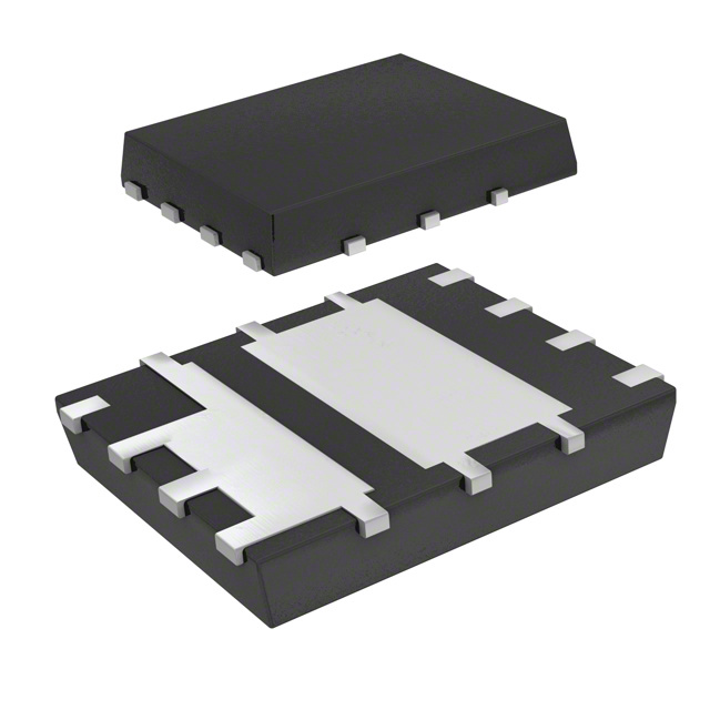
The AONY36356 is a 30V dual asymmetric N-channel MOSFET manufactured by Alpha & Omega Semiconductor Inc. utilizing Trench Power MOSFET technology. It features two independent channels in an 8-DFN (5x6) package with exposed pad. Q1 provides a maximum on-resistance of 6.1mΩ at VGS=10V and 9.6mΩ at VGS=4.5V, with a continuous drain current of 32A. Q2 offers lower resistance at 3.8mΩ (10V) and 4.7mΩ (4.5V), supporting 32A continuous current. The device includes 100% UIS and Rg testing, operates within -55°C to 150°C junction temperature, and complies with RoHS standards.
Verify the specific ordering suffix against the manufacturer's official documentation to confirm package type and tape/reel specifications. Ensure compliance with applicable export control regulations and legal requirements before procurement. Confirm that the component meets RoHS and halogen-free standards as stated in the datasheet.
Select this component when designing asymmetric power stages where one channel requires significantly lower on-resistance than the other. Evaluate thermal performance using the provided junction-to-case and junction-to-ambient thermal impedance curves. Verify that the gate charge requirements align with the driving circuit capabilities for both 4.5V and 10V logic levels.
This part belongs to Alpha & Omega Semiconductor's portfolio of trench power MOSFETs designed for efficient power management. The company specializes in power integrated circuits and discrete semiconductors for computing, telecommunications, and industrial applications. The AONY series focuses on providing optimized solutions for modern power conversion topologies.
Consult the manufacturer's datasheet for similar parts such as the AONP36336 or AONY36352. Verify pinout compatibility and electrical parameters before substitution. Ensure any replacement maintains the required asymmetric characteristics and thermal performance.
Q1 has a higher on-resistance (max 6.1mΩ at 10V) compared to Q2 (max 3.8mΩ at 10V). This asymmetry allows designers to use different channels for distinct load requirements within a single package.
Yes, the datasheet specifies that every unit undergoes 100% Unclamped Inductive Switching (UIS) testing to ensure reliability under inductive load conditions.
The absolute maximum rating for Gate-Source Voltage (VGS) is ±12V. Exceeding this limit may damage the device.
 AONY36356
The activity of extra discounts on wholesale prices is in full swing…
Please fill in your contact information and we will send you the latest wholesale price list.