ChipApex | Global Electronic Components Supplier
SEARCH
Search Product
Search Post
— IC芯片 | 连接器 | 传感器 | 被动器件 —
Search productSearch post
— IC芯片 | 连接器 | 传感器 | 被动器件 —
Consult the customer manager about the wholesale price.
consultation hotline:86-132-6715-2157
email:[email protected]
Contact the product manager for consultation. One-stop consultation is available.
Do you want a lower wholesale price? Please send us your inquiry and we will reply immediately.
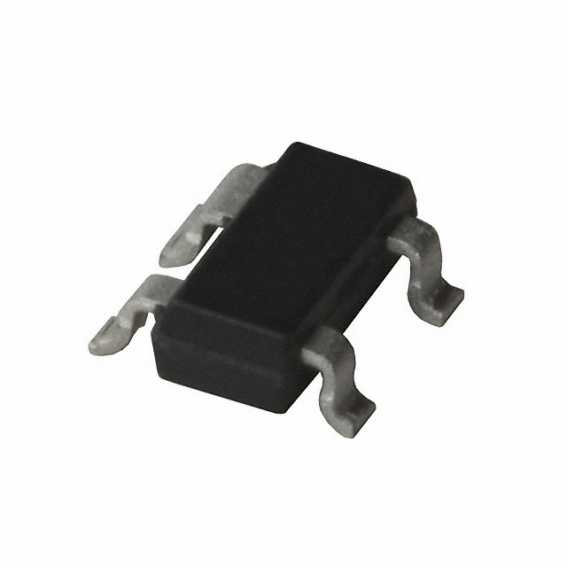
The AT-32011-TR1G is a high-performance NPN silicon bipolar transistor designed for low current and low voltage operation. It utilizes a self-aligned-transistor process with nitride passivation to achieve excellent uniformity and reliability. The device features a 4-lead SOT-143 package, offering superior RF performance compared to the 3-lead variant. Key electrical specifications include a collector-emitter breakdown voltage (VCEO) of 5.5 V, an emitter-base breakdown voltage (VEBO) of 1.5 V, and a maximum collector current (IC) of 32 mA. At 2.7 V and 2 mA bias, it delivers a minimum forward current transfer ratio (hFE) of 70.
Verify the specific ordering suffix when purchasing. The 'TR1' designation indicates a 7-inch reel quantity of 3000 units. The 'G' suffix denotes a lead-free option. Confirm compatibility with high-volume surface mount assembly techniques required by your manufacturing line.
Select this component for designs requiring high gain and low noise figures at low supply voltages. The 4-lead SOT-143 package is preferred over the 3-lead alternative for better RF performance. Ensure bias conditions align with the specified test parameters for optimal noise figure and associated gain characteristics.
This part belongs to the Agilent/Broadcom AT-3 series of low-current, high-performance NPN bipolar transistors. It shares the same die technology as the AT-32033 but differs in packaging. The AT-32011 specifically uses the 4-lead SOT-143 package to enhance performance metrics compared to the industry-standard SOT-23 package used by its counterpart.
The AT-32033 is the functional equivalent using the same die but housed in a 3-lead SOT-23 package. Substitution requires accounting for the difference in pinout and thermal resistance between the SOT-143 and SOT-23 packages.
The AT-32011 uses a 4-lead SOT-143 package which offers higher performance than the 3-lead SOT-23 package used by the AT-32033, despite both utilizing the same die.
The device is optimized for performance at 2.7 V, making it ideal for end-of-life battery use in wireless applications.
It is fabricated using an optimized version of Agilent’s 10 GHz ft, 30 GHz fMAX Self-Aligned-Transistor (SAT) process with ion-implantation and gold metalization.
 AT-32011-TR1
The activity of extra discounts on wholesale prices is in full swing…
Please fill in your contact information and we will send you the latest wholesale price list.