 ChipApex | Global Electronic Components Supplier
SEARCH
Search Product
Search Post
— IC芯片 | 连接器 | 传感器 | 被动器件 —
Search productSearch post
— IC芯片 | 连接器 | 传感器 | 被动器件 —
Consult the customer manager about the wholesale price.
consultation hotline:86-132-6715-2157
email:[email protected]
Contact the product manager for consultation. One-stop consultation is available.
Do you want a lower wholesale price? Please send us your inquiry and we will reply immediately.
The AT-32033-TR1 is an NPN silicon bipolar transistor from the Agilent AT-3 series, optimized for low current and low voltage operation. It utilizes a self-aligned-transistor process with nitride passivation and gold metalization. The device features a 3.2-micron emitter-to-emitter pitch and a 20-finger interdigitated geometry to minimize parasitics. It is housed in a standard SOT-23 surface-mount package. Key electrical specifications include a collector-emitter breakdown voltage of 5.5 V, an emitter-base breakdown voltage of 1.5 V, and a maximum collector current of 32 mA. Power dissipation is rated at 200 mW, with a junction temperature range spanning -65°C to +150°C.
Verify the exact ordering suffix against official documentation before procurement. The 'TR1' designation indicates a specific tape-and-reel packaging format containing 3000 devices on a 7-inch reel. Confirm lead-free availability requirements by checking if a 'G' suffix is necessary for the final part number. Ensure compatibility with high-volume surface mount assembly techniques during integration planning.
Select this component when designing circuits requiring high gain and low noise figures at low bias currents. It is particularly suitable for 900 MHz, 1.8 GHz, and 2.4 GHz bands. Consider the SOT-23 package constraints regarding thermal dissipation and pinout compatibility with existing PCB footprints. Evaluate performance at 2.7 V for end-of-life battery scenarios versus higher voltage operation.
This component belongs to the Agilent AT-3 series of low-current, high-performance NPN silicon bipolar transistors. The series shares identical die technology but differs in packaging; the AT-32011 variant uses a four-lead SOT-143 package for enhanced performance, while the AT-32033 utilizes the three-lead SOT-23 package. Both are fabricated using the same 10 GHz ft, 30 GHz fMAX self-aligned process.
The AT-32011 serves as a functional alternative within the same family, offering similar electrical characteristics but housed in a four-lead SOT-143 package instead of the SOT-23. Designers must account for the physical footprint differences and potential pinout variations when substituting between these two models.
At a frequency of 0.9 GHz with a collector-emitter voltage of 2.7 V and a collector current of 2 mA, the typical minimum noise figure is 1.0 dB.
Associated gain increases with higher bias currents. At 2 mA, the gain is approximately 12.5 dB, while at 20 mA, it rises to approximately 15 dB under optimal tuning conditions at 0.9 GHz.
Yes, the device has a collector-emitter breakdown voltage (VCEO) of 5.5 V, making it suitable for operation at 5 volts despite being optimized for lower voltage battery applications.
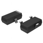 AT-32033-TR1
The activity of extra discounts on wholesale prices is in full swing…
Please fill in your contact information and we will send you the latest wholesale price list.





