 ChipApex | Global Electronic Components Supplier
SEARCH
Search Product
Search Post
— IC芯片 | 连接器 | 传感器 | 被动器件 —
Search productSearch post
— IC芯片 | 连接器 | 传感器 | 被动器件 —
Consult the customer manager about the wholesale price.
consultation hotline:86-132-6715-2157
email:[email protected]
Contact the product manager for consultation. One-stop consultation is available.
Do you want a lower wholesale price? Please send us your inquiry and we will reply immediately.
The AT17C256-10SC is a 256K-bit (262,144 x 1-bit) serial EEPROM designed for FPGA configuration. It operates at 5V nominal and supports industrial temperature ranges (-40°C to +85°C). The device features a simple 2-wire serial interface for in-system programming and utilizes a master serial mode to automatically load configuration programs into FPGAs upon power-up. It includes programmable reset polarity, write protection, and cascading capabilities via the CEO output.
Verify that the specific ordering suffix corresponds to the required package type and operating temperature range. Confirm compatibility with the target FPGA's master serial mode requirements. Ensure the supply voltage matches the 5V nominal specification for the AT17C variant. Check for any legacy status or obsolescence notices from the manufacturer.
Select this component when a non-volatile memory solution is required for FPGA configuration in industrial environments. It is suitable for designs requiring cascading capabilities to expand memory capacity beyond single-device limits. Consider the 8-pin SOIC package for space-constrained surface-mount applications. Verify interface compatibility with the specific FPGA model being configured.
This part belongs to the low-density AT17 Series of FPGA Configuration EEPROMs. The family includes 64K, 128K, and 256K bit densities. The 'C' designation indicates 5V operation, while 'LV' denotes 3.3V versions. These devices serve as configurators, providing cost-effective and easy-to-use memory solutions for various FPGA architectures.
AT17LV256-10SC
The device supports two connection conditions for the RESET/OE pin. If driven by the FPGA CON pin, it may lose sync during external resets unless the reset polarity is programmed active High. Alternatively, driving RESET/OE from the FPGA RESET input clears the address pointer, ensuring reconfiguration starts correctly.
The Chip Enable Output (CEO) pin is asserted Low on the clock cycle following the last bit read from the memory. This signal enables cascading by allowing the next EEPROM in the chain to enable its data output driver.
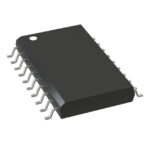 AT17C256-10SC
The activity of extra discounts on wholesale prices is in full swing…
Please fill in your contact information and we will send you the latest wholesale price list.




