 ChipApex | Global Electronic Components Supplier

SEARCH
Search Product
Search Post
— IC芯片 | 连接器 | 传感器 | 被动器件 —
Search productSearch post
— IC芯片 | 连接器 | 传感器 | 被动器件 —
Consult the customer manager about the wholesale price.
consultation hotline:86-132-6715-2157
email:[email protected]
Contact the product manager for consultation. One-stop consultation is available.
Do you want a lower wholesale price? Please send us your inquiry and we will reply immediately.
AT17LV256A-10JI is listed in the Configuration PROMs For FPGAs range at ChipApex. The manufacturer field lists Microchip Technology. Its product description is IC SRL CONFG EEPROM 256K 20-PLCC. Review the specifications below when checking this part for your BOM.
The AT17LV256A-10JI is a 256-Kbit (32K x 8) serial EEPROM designed for FPGA configuration. It operates at a maximum clock frequency of 10 MHz and supports supply voltages of 3.0V to 3.6V or 4.5V to 5.5V. The device features in-system programmability via a 2-wire bus, low-power standby mode, and high endurance of 100,000 write cycles with 90-year data retention. It is housed in a 20-lead PLCC package and functions within an industrial temperature range of -40°C to +85°C.
Verify the specific ordering suffix against the manufacturer's current datasheet to confirm package type and voltage tolerance. Ensure the industrial temperature grade (-40°C to +85°C) matches the application requirements. Confirm that the 20-lead PLCC footprint aligns with the target PCB design. Check for any recent revisions to the pinout or electrical characteristics before finalizing procurement.
Select this component when a cost-effective, serial-access configuration memory is required for SRAM-based FPGAs. It is suitable for designs needing in-system programmability without external controllers. Consider the 256-Kbit density for smaller FPGA configurations or as part of a cascaded chain for larger arrays. Verify power supply constraints to ensure compatibility with either 3.3V or 5V system architectures.
This device belongs to the AT17A series of FPGA configurators, which are specialized EEPROMs optimized for loading configuration programs into field-programmable gate arrays. The series offers various densities from 64-Kbit to 2-Mbit, sharing pin-compatible packages across the family. These devices simplify the configuration process by interfacing directly with FPGA control signals, eliminating the need for complex external programming hardware during normal operation.
AT17LV256A-10JC
The device uses its nCASC output pin to signal the completion of data transfer. This pin connects to the nCS input of the next configurator in the chain, allowing subsequent devices to begin outputting data automatically.
Yes, the user can program the polarity of the RESET/OE pin to be either active-high or active-low during the programming phase to match specific FPGA requirements.
During FPGA loading operations, the SER_EN pin must be held High. It is only driven Low to enter the 2-wire Serial Programming Mode for in-system programming.
Explore related parts through Memory, Integrated Circuits (ICs), all product categories, ChipApex homepage.
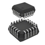 AT17LV256A-10JI

The activity of extra discounts on wholesale prices is in full swing…
Please fill in your contact information and we will send you the latest wholesale price list.





