ChipApex | Global Electronic Components Supplier
SEARCH
Search Product
Search Post
— IC芯片 | 连接器 | 传感器 | 被动器件 —
Search productSearch post
— IC芯片 | 连接器 | 传感器 | 被动器件 —
Consult the customer manager about the wholesale price.
consultation hotline:86-132-6715-2157
email:[email protected]
Contact the product manager for consultation. One-stop consultation is available.
Do you want a lower wholesale price? Please send us your inquiry and we will reply immediately.
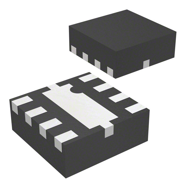
The ATF-511P8 is a high linearity enhancement mode pseudomorphic HEMT housed in an 8-lead JEDEC-standard leadless plastic chip carrier (LPCC) package measuring 2.0 x 2.0 x 0.75 mm. It operates from 50 MHz to 6 GHz with single positive Vgs biasing, eliminating the need for negative gate voltage. At 2 GHz with Vds = 4.5V and Ids = 200 mA, it delivers a typical output IP3 of 41.7 dBm, P1dB of 30 dBm, noise figure of 1.4 dB, gain of 14.8 dB, and PAE of 69%. The device features excellent uniformity, point MTTF exceeding 300 years at +85°C mounting temperature, MSL-1 rating, and lead-free construction.
Verify the specific ordering suffix against the manufacturer's current documentation to confirm container type and quantity. The datasheet lists ATF-511P8-TR1 as a 3000-unit 7-inch reel and ATF-511P8-TR2 as a 10000-unit 13-inch reel. Confirm that the component meets RoHS compliance requirements if applicable to your design specifications before finalizing procurement.
Select this component when designing circuits requiring high linearity and low noise in a compact form factor. Ensure the bias network supports the required Vds and Ids levels for optimal OIP3 and P1dB performance. Consider the thermal resistance characteristics and PCB land pattern guidelines provided in the datasheet to maintain channel temperature within safe operating limits during continuous RF drive conditions.
The ATF-511P8 belongs to the family of pseudomorphic HEMT devices designed for RF power amplification. Manufactured originally by Avago Technologies, which was later acquired by Broadcom Inc., this component represents a standard solution for medium-power amplification tasks in wireless communication systems. The device utilizes enhancement mode technology to simplify biasing requirements compared to conventional depletion mode devices.
Public confirmed substitute part numbers are not available in the provided documentation. Verify compatibility with existing circuit designs if considering alternative manufacturers or updated generations of similar RF transistors.
The operational gate voltage ranges from 0.25 V to 0.8 V when biased at Vds = 4.5V and Ids = 200 mA.
The device features backside metalization in its 2x2 mm LPCC package, providing excellent thermal dissipation capabilities and visual evidence of solder reflow.
The device can safely handle +30 dBm RF input power, provided the gate current (Igs) is limited to 46 mA.
 ATF-511P8-TR1
The activity of extra discounts on wholesale prices is in full swing…
Please fill in your contact information and we will send you the latest wholesale price list.