 ChipApex | Global Electronic Components Supplier
SEARCH
Search Product
Search Post
— IC芯片 | 连接器 | 传感器 | 被动器件 —
Search productSearch post
— IC芯片 | 连接器 | 传感器 | 被动器件 —
Consult the customer manager about the wholesale price.
consultation hotline:86-132-6715-2157
email:[email protected]
Contact the product manager for consultation. One-stop consultation is available.
Do you want a lower wholesale price? Please send us your inquiry and we will reply immediately.
The AUIRF7309Q is an automotive-grade dual HEXFET power MOSFET in an SO-8 package, integrating N-channel and P-channel devices. It features a 30V drain-source breakdown voltage (VDSS) with a maximum on-resistance (RDS(on)) of 0.05Ω for the N-channel at VGS=10V and 0.10Ω for the P-channel at VGS=-10V. Continuous drain currents are 4.0A (N-Ch) and -3.0A (P-Ch) at TA=25°C. The device supports a junction temperature up to 150°C, operates with logic-level gate drive, and includes dynamic dv/dt ratings for ruggedized performance.
Verify the specific ordering suffix when purchasing. The base part number AUIRF7309Q corresponds to the standard tape and reel form factor containing 4000 units. Confirm that the received components match the SO-8 package outline and pinout diagram provided in the datasheet to ensure compatibility with your PCB footprint and assembly process.
Select this component for designs requiring integrated N and P channel switching in a small footprint. Ensure the thermal design accounts for the junction-to-ambient resistance of 90°C/W under steady-state conditions. Verify that the gate drive voltage meets the logic level requirements for optimal RDS(on) performance and check that the continuous current demands do not exceed the rated limits at the expected ambient temperature.
This device belongs to Infineon's HEXFET family of power MOSFETs, specifically engineered for automotive reliability. It utilizes advanced processing techniques to minimize on-resistance while maintaining fast switching speeds. The dual-channel design simplifies circuit topology by combining complementary switches into one component, reducing board space and assembly complexity compared to discrete solutions.
No public confirmed substitute part numbers are listed in the documentation. Engineers should verify pin compatibility and electrical parameters before considering alternative manufacturers or different part numbers from the same supplier.
The N-channel has a peak diode recovery dv/dt rating of 6.9 V/ns, while the P-channel is rated at 6.0 V/ns.
Yes, the device is qualified for automotive applications and supports an operating junction temperature range up to 150°C.
The total gate charge for the N-channel is typically 25 nC under test conditions of ID = 2.6A, VDS = 16V, and VGS = 4.5V.
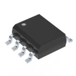 AUIRF7309Q
The activity of extra discounts on wholesale prices is in full swing…
Please fill in your contact information and we will send you the latest wholesale price list.





