ChipApex | Global Electronic Components Supplier
SEARCH
Search Product
Search Post
— IC芯片 | 连接器 | 传感器 | 被动器件 —
Search productSearch post
— IC芯片 | 连接器 | 传感器 | 被动器件 —
Consult the customer manager about the wholesale price.
consultation hotline:86-132-6715-2157
email:[email protected]
Contact the product manager for consultation. One-stop consultation is available.
Do you want a lower wholesale price? Please send us your inquiry and we will reply immediately.
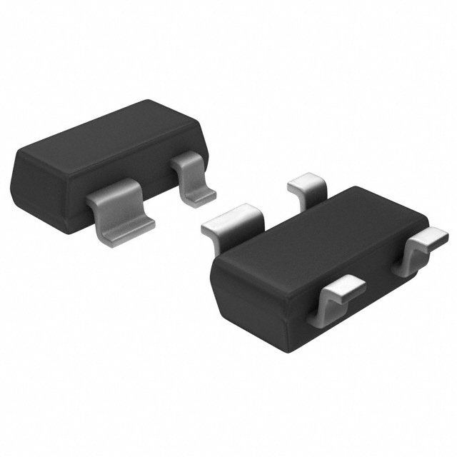
The BF991 is an N-channel dual-gate depletion-type MOS-FET in a SOT143 microminiature package. It features integrated back-to-back diodes between gates and source for surge protection. Key electrical parameters include a drain-source voltage of 20 V, a drain current of 20 mA, and total power dissipation of 200 mW up to 60 °C. The device exhibits a transfer admittance of 14 mS at 1 kHz and a noise figure of 1.2 dB at 200 MHz.
Verify the specific revision status (Rev. 03) against the latest NXP documentation before finalizing designs. Confirm that the SOT143 package dimensions and pinout align with the target PCB footprint requirements. Ensure thermal management strategies account for the specified junction-to-ambient resistance and derating curves under expected operating temperatures.
Select this component for VHF frequency applications requiring low noise figures and high gain stability. The dual-gate configuration allows for independent control of input impedance and gain, making it suitable for tuner stages. Consider the 20 V drain-source voltage limit when designing biasing circuits for RF signal amplification.
This part is an N-channel dual-gate MOS-FET designed for RF front-end applications. It belongs to the category of depletion-mode field-effect transistors used in analog signal processing. The SOT143 package provides a compact form factor suitable for space-constrained consumer electronics and professional communication hardware.
No public confirmed substitute part numbers are available in the provided documentation.
 BF991,215
The activity of extra discounts on wholesale prices is in full swing…
Please fill in your contact information and we will send you the latest wholesale price list.