 ChipApex | Global Electronic Components Supplier
SEARCH
Search Product
Search Post
— IC芯片 | 连接器 | 传感器 | 被动器件 —
Search productSearch post
— IC芯片 | 连接器 | 传感器 | 被动器件 —
Consult the customer manager about the wholesale price.
consultation hotline:86-132-6715-2157
email:[email protected]
Contact the product manager for consultation. One-stop consultation is available.
Do you want a lower wholesale price? Please send us your inquiry and we will reply immediately.
The BFG424W is an NPN double polysilicon wideband transistor with a buried layer, designed for low voltage applications in a plastic SOT343R package. Key electrical parameters include a collector-base voltage (VCBO) of 10 V and a collector-emitter voltage (VCEO) of 4.5 V. The maximum collector current is 30 mA, with total power dissipation rated at 135 mW. It features a transition frequency (fT) of 25 GHz and a maximum power gain (Gp(max)) of 22 dB at 2 GHz. Noise figure is typically 1.2 dB at 2 GHz.
Verify the component status before procurement, as the product may be listed as no longer manufactured. Confirm the specific ordering suffix matches the required tape reel configuration. Ensure ESD precautions are observed during handling due to device sensitivity. Cross-reference the marking code ND* to validate authenticity against official datasheets.
Select this component for low voltage RF wideband applications requiring high transition frequency and low noise figure. Verify that the operating conditions remain within the absolute maximum ratings, specifically the 4.5 V collector-emitter voltage limit. Consider the SOT343R package dimensions and reverse pinning when designing PCB footprints. Evaluate thermal resistance requirements based on the emitter solder point temperature constraints.
The BFG424W is part of NXP Semiconductors' portfolio of NPN double polysilicon wideband transistors. It utilizes a buried layer structure optimized for low voltage performance. The device is housed in a compact SOT343R surface-mounted package with four leads. This series targets high-frequency communication systems where small form factor and efficient heat dissipation through the emitter are critical design factors.
Consult official replacement lists or cross-reference databases for verified substitutes. Ensure any alternative component matches the SOT343R package and electrical specifications. Verify compatibility with existing circuit designs before implementation.
The maximum collector-emitter voltage (VCEO) with an open base is 4.5 V.
The emitter acts as the thermal lead, and the total power dissipation rating depends on the temperature at the soldering point of the emitter pins.
The typical noise figure is 1.2 dB at 2 GHz with a collector current of 2 mA and VCE of 2 V.
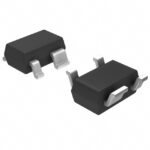 BFG424W,115
The activity of extra discounts on wholesale prices is in full swing…
Please fill in your contact information and we will send you the latest wholesale price list.






