 ChipApex | Global Electronic Components Supplier
SEARCH
Search Product
Search Post
— IC芯片 | 连接器 | 传感器 | 被动器件 —
Search productSearch post
— IC芯片 | 连接器 | 传感器 | 被动器件 —
Consult the customer manager about the wholesale price.
consultation hotline:86-132-6715-2157
email:[email protected]
Contact the product manager for consultation. One-stop consultation is available.
Do you want a lower wholesale price? Please send us your inquiry and we will reply immediately.
The BFR505 is an NPN silicon planar epitaxial transistor designed for RF front-end wideband applications in the GHz range. It features a transition frequency of 9 GHz and a collector-emitter voltage rating of 15 V. The device operates with a DC collector current up to 18 mA and supports a total power dissipation of 150 mW at a soldering point temperature of 135 °C. Key electrical characteristics include a typical DC current gain (hFE) of 120, a maximum unilateral power gain of 17 dB at 900 MHz, and a noise figure ranging from 1.2 dB to 2.1 dB depending on bias conditions. Encapsulated in a plastic SOT-23 package, it utilizes gold metallization for reliability.
Verify the component authenticity by checking the marking code '31*' against the manufacturer's documentation. Confirm the package type is SOT-23 and ensure the ordering suffix matches the specific tape-and-reel configuration required for your assembly process. Cross-reference the revision history to ensure the datasheet version aligns with the production batch specifications.
Select this component for wideband RF applications requiring high transition frequency and low noise. Ensure the design accommodates the 15 V collector-emitter voltage limit and 150 mW power dissipation constraints. Verify that the operating junction temperature remains within the specified limits and that the biasing circuit provides the recommended 5 mA collector current for optimal gain and noise performance.
The BFR505 is part of NXP Semiconductors' discrete transistor portfolio, specifically engineered for radio frequency and wideband applications. It serves as a key active component in mobile communication devices and satellite reception systems where high-frequency performance and signal fidelity are critical requirements.
Consult official NXP documentation for qualified substitute part numbers. Ensure any replacement maintains compatibility with the SOT-23 package and meets or exceeds the 9 GHz transition frequency and 15 V voltage ratings.
The maximum unilateral power gain is typically 17 dB when measured at IC = 5 mA, VCE = 6 V, and Tamb = 25 °C.
At f = 900 MHz, the noise figure ranges from 1.2 dB to 1.7 dB at IC = 1.25 mA, and from 1.6 dB to 2.1 dB at IC = 5 mA.
The thermal resistance Rth(j-s) from junction to soldering point is typically 260 K/W.
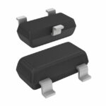 BFR505,215
The activity of extra discounts on wholesale prices is in full swing…
Please fill in your contact information and we will send you the latest wholesale price list.





